- Semiconductor BusinessHOME
- Products and Services of Macnica,Inc.
-
technical information

-
Events and Seminars
- Handling Manufacturer
- Support
- Inquiry
- Click here to purchase products
- Semiconductor business e-mail magazine registration
![]()
![]() Narrow down by specifying conditions
Narrow down by specifying conditions
現在2183件がヒットしています。check
*Notice: The following video content has been updated for the latest tool environment.
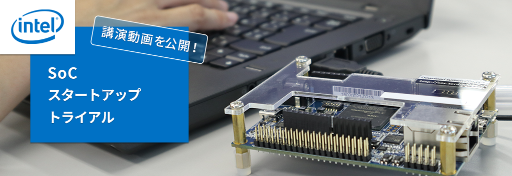
"SoC Startup Trial" released in video! - Semiconductor business -Macnica (macnica.co.jp)
If you are using an older version (v18.1 or earlier) of the development environment, please refer to the video on the old page from the link above.
Purpose of this course
Overview
The presentation of the popular hands-on seminar "SoC Startup Trial" has been released as an online video.
This seminar introduces the Intel® SoC development flow for customers who are considering Intel® SoC FPGA development for the first time. The original seminar is a hands-on seminar where you can experience and learn the actual development flow using Quartus® Prime/Platform Designer and Intel® SoC FPGA Embedded Development Suite (SoC EDS). Intel® SoC FPGA Seminar in a Box” evaluation kit free rental service, and a separate exercise manual “SoC Beginner's Guide - SoC Simple Tutorial (Atlas-SoC / DE10-Nano Board Version)” can also be used to experience the hands-on content.
The main target of this seminar is Cyclone® V SoC / Arria® V SoC. If you are using a SoC FPGA from another device family, please understand that there are differences in device specifications and tool usage.
Target audience
・System, H/W, S/W designers who are interested in Intel® SoC FPGA
・People who are considering starting development using Intel® SoC FPGA
- As an introduction to developing with Intel® SoC FPGAs
goal of attending
・Understanding the overview and structure of Intel® SoC FPGA devices
・Development environment: Understanding of Intel® SoC FPGA Embedded Development Suite (SoC EDS)
・Understanding of development flow using Intel® SoC FPGA
- Hardware development flow (HPS option setting on Platform Designer)
- Software development flow (bootloader generation, HWLib, how to use various tools)
- How hardware design and software design work together (handoff mechanism)
agenda
| No. | title | required time |
| 1 |
Overview of SoC FPGAs |
11 minutes 33 seconds |
| 2 |
Configuration and boot, system development flow |
4 minutes 2 seconds |
| 3 |
Hardware Design Flow (1/2) Platform Designer Overview, Project Creation ~ |
14 minutes 15 seconds |
| 4 |
Hardware design flow (2 of 2) HPS component configuration |
10 minutes 38 seconds |
| 5 |
Software Development Environment - SoC EDS Overview |
10 minutes 26 seconds |
| 6 |
Software Design Flow (1/3) - Design Flow Overview, Bootloader |
10 minutes 06 seconds |
| 7 |
Software Design Flow (2 of 3) - Baremetal/RTOS Based Applications |
10 minutes 49 seconds |
| 8 |
Software design flow (3/3) - other tools provided |
6 minutes 42 seconds |
| 9 |
Introducing RocketBoards.org - The Linux Community Portal |
2 minutes 40 seconds |
Seminar content
SoC FPGA overview, system architecture

This chapter introduces the Intel® SoC FPGA product lineup, device overview, and system architecture.
(Duration: 11 minutes 33 seconds)
Configuration and boot, system development flow

This chapter introduces the configuration and boot methods and the system development flow.
(Duration: 4 minutes 2 seconds)
Hardware design flow (1/2) project generation ~

This chapter covers the following items in the hardware design flow:
・Overall flow of hardware design (creation of project ~)
・Platform Designer functions and how to use them
・Mechanism of register address determination on the FPGA side as seen from ARM
(Duration: 14 minutes 15 seconds)
Hardware design flow (2 of 2) HPS component configuration

This chapter covers the following items in the hardware design flow:
・HPS component option setting items
- Interface setting with FPGA side
- HPS peripheral selection and pinout
- HPS side clock setting, SDRAM controller setting
(Duration: 10 minutes 38 seconds)
Software Development Environment - SoC EDS Overview

This chapter introduces the editions and offerings of the Intel® SoC FPGA Embedded Development Suite provided as a software development environment.
(Duration: 10 minutes 26 seconds)
Software Design Flow (1/3) - Design Flow Overview, Bootloader

This chapter covers the following items in the software design flow:
・Overview of software development environment
・How to generate a bootloader (Preloader)
・HPS boot sequence
(Required time: 10 minutes 06 seconds)
Software Design Flow (2 of 3) - Baremetal/RTOS Based Applications

This chapter covers the following items in the software design flow:
・HWLib library, sample projects
・Debugger script
・Arm DS operation (creating a project to debugging)
・Flash writing tool (HPS Flash Programmer)
(Duration: 10 minutes 49 seconds)
Software design flow (3/3) - other tools provided

This chapter covers the following items in the software design flow:
・How to create a system header file
・バイナリー変換、ヘッダー付加
・Flash writing tool (HPS Flash Programmer)
(Duration: 06 minutes 42 seconds)
Introducing RocketBoards.org - The Linux Community Portal

This chapter introduces RocketBoards.org, a community site that publishes information related to Linux and open source software.
(Duration: 02 minutes 40 seconds)
Other recommended information
Exercise content (for those who want to experience hands-on)
Introduction to Intel® Official FPGA Training (for those who are considering courses other than this seminar)
See below for a list of distributor-sponsored technical trainings and seminars on Intel® FPGA products.
Intel FPGA Seminar & Training Top Page
Find official Intel® online training in the training catalog below.
Intel® FPGA Technical Training Catalog
Intel® SoC FPGA Information Summary Page
The following pages contain links to SoC FPGA-related articles/materials and samples.
Click here for recommended articles/materials
SoC FPGA related articles and resources
Intel® FPGA Development Flow/FPGA Top Page