- Semiconductor BusinessHOME
- Products and Services of Macnica,Inc.
-
technical information

-
Events and Seminars
- Handling Manufacturer
- Support
- Inquiry
- Click here to purchase products
- Semiconductor business e-mail magazine registration
![]()
![]() Narrow down by specifying conditions
Narrow down by specifying conditions
現在2004件がヒットしています。check

In the 10th episode, we will "introduce the layout method when designing an FPGA power supply circuit"!
Basically, refer to the Gerber data on the evaluation board for any power supply. Please refer to the data sheet only for explanations of layout precautions. Please note that the layout on the datasheet may be simplified.
|
Step 1: Check the schematic
First, in preparation, check the circuit diagram. Prepare the circuit diagram from the data sheet and the demo board circuit diagram, and also search for a circuit diagram that matches your desired specifications. If you do not have a circuit diagram with the desired voltage settings, complete the power supply circuit by determining the peripheral constants based on the calculation formula in the data sheet.
Step 2: Power supply circuit design including FPGA
Next, we will modify the circuit diagram to suit your application. This is the circuit design of the entire power line that connects the power circuit and FPGA. We also design the FPGA power supply sequence.
- Reflects output voltage settings, output voltage slope at startup, Enable operation method, device-specific function settings, etc.
- In the FPGA power supply design, the capacitance calculated by the PDN tool is also reflected.
- Use the EPE to calculate and reflect the output voltage setting.
- It also considers sequences such as Enable.
Step 3: Prepare layout and check precautions
Check the Gerber data of the power supply circuit evaluation board and create a layout for the power supply circuit alone. Please carefully check the notes on the data sheet for layout precautions.
Figure 1 is the recommended layout for Analog Devices' μModule LTM4650. Next to it are some notes on the layout in the datasheet. Using this as a reference, use CAD to design the layout of the power supply circuit.
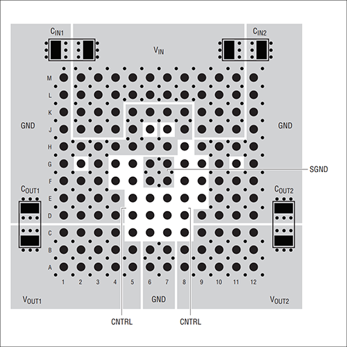
**** Layout notes *****
• Connect input and output high frequency ceramic capacitors to VIN,
Placed adjacent to the PGND and VOUT pins for high frequency
Minimize noise.
• Place the ground layer on the second layer.
• Minimize via conduction losses and reduce module thermal stress.
interconnections between the top layer and other power layers to reduce
Then use a large number of vias.
• Over pads unless they are filled or plated vias.
Do not place vias directly.
• Separate SGND ground copper area for components connected to signal pins.
use. Connect SGND and GND under the device.
Step 4: Board design
We design circuits and boards that take into consideration not only power devices, but also FPGAs and other peripheral devices.
When placing a bead filter between the power supply circuit and the FPGA, care must be taken to avoid placing the filter within the power supply feedback loop. Also, if an IR drop occurs due to the filter, it may deviate from the power supply voltage accuracy required by the FPGA, so please consider reviewing the voltage setting constants.
If you think that the voltage accuracy required by the FPGA cannot be met, consider a power system management device that has a remote sensing function for the power supply or a servo function to improve the accuracy of the power supply voltage.
Step 5: Design verification
After this, we will verify the board design.
If possible, we recommend that you use SI/PI simulation to confirm that the FPGA power supply circuit design is as desired. If you run an SI/PI simulation and find a problem with the quality of the power supply, repeat steps 2 to 5 to prevent problems in your design.
Step 6: Board production and actual device verification
Once you have repeated steps 2 to 5 until you have what you think is the optimal board design, you can proceed with manufacturing the board.
Finally, we would like you to perform a test on the actual machine and confirm that there are no problems.
Click here for an overview of μModule🄬 used in Intel evaluation boards>>