- Semiconductor BusinessHOME
- Products and Services of Macnica,Inc.
-
technical information

-
Events and Seminars
- Handling Manufacturer
- Support
- Inquiry
- Click here to purchase products
- Semiconductor business e-mail magazine registration
![]()
![]() Narrow down by specifying conditions
Narrow down by specifying conditions
現在2168件がヒットしています。check


In this column, we will introduce "technical information on FPGA that is surprisingly unknown, but makes a difference if you know it."
From FPGA beginners to veterans, the contents can be used widely, so please keep in touch with us until the end.
【第 5 回】 これが究極の低消費電力手法?
The low power consumption design method is an accumulation of detailed measures.
Rather than memorizing detailed measures, it is important to understand the power consumption calculation formula and the parameters used in it, and to design with an awareness of power consumption on a regular basis.
Until now, even if you thought it was troublesome to understand the calculation formula, we recommend that you take a look at the calculation formula once.
I think you can get a quicker understanding by looking at which parameters the low power techniques you know affect.
1.1 CMOS回路の消費電力計算式
| power consumption | = | dynamic power + leakage power |
| = | [switching power + short circuit power] + leakage power | |
| = | [0.5*(C*Vs*VCC*F)*N] + [Q*VCC*F*N] + [(Idc+Ileak)*VCC] |
| C:負荷容量 |
| Vs:信号振幅 |
| VCC:電源電圧 |
| F:動作周波数 |
| N:信号遷移頻度(トグル率) |
| Q:貫通電流による電荷 |
| Idc:回路固有のDC電流 |
| Ileak:リーク電流 |
1.1.1 ダイナミック電力
信号が遷移した時の電力で、スイッチング電力とショートサーキット(貫通)電力の合計です。
(1) スイッチング電力
セルが動作して、負荷容量を充放電した際に消費する電力の事です。
負荷容量は、配線容量と次のセルの入力ピン容量の合計です。
例えば、インバーターの入力に ”L” を入力すると pMOS が ”ON”、nMOS が ”OFF” になり、VCC から電流が流れて、配線や次段の入力ピンの容量を充電します。この時に pMOS の抵抗により電力を消費します。
次に、インバーターの入力に ”H” を入れると pMOS が “OFF”、nMOS が ”ON” になり、負荷容量に充電された電荷が nMOS を通って GND へ流れます。この時に nMOS の抵抗により電力を消費します。
この容量は、配線抵抗と次段セルの入力ピン容量の合計となり、配線が長く Fanout が大きいとスイッチング電力が増加します。
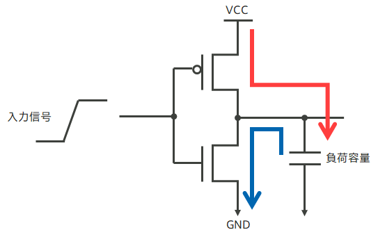
(2) ショートサーキット電力
CMOS は入力信号が ”L” か ”H” で安定していれば、pMOS か nMOS のどちらかが必ず OFF になり、リーク電流を除き VCC から GND へ電流が流れません。
CMOS が低消費電力と言われてる理由です。しかし、入力信号の立上りや立下りが鈍いと、一時的に pMOS と nMOS が両方共に少し開いた ON 状態になります。
この時に、VCC から GND へショートサーキット電流が流れ、この電力をショートサーキット電力と言います。
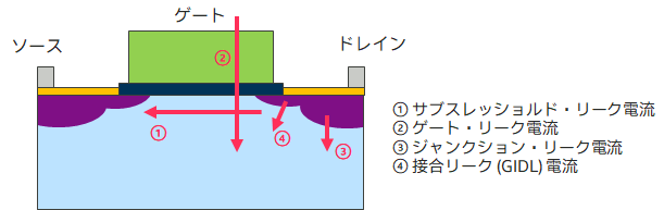
1.1.2 Leakage power
Leakage power is the power transmitted by the following four types of leakage currents.
While the old process had a negligible value, the newer process had significantly higher leakage power.
These leakage powers are consumed regardless of operation if voltage is applied to the transistor.
Subthreshold leakage current and gate leakage current dominate today.
Since the subthreshold leakage current is highly dependent on temperature, leakage power increases further at higher temperatures.
|
kinds |
Contents |
Cause |
Temperature Dependence |
| サブスレッショルドリーク電流 (ソース-ドレイン・リーク) |
トランジスタがOFF状態でソースとドレイン間に流れる電流 | トランジスタのVt(閾値電圧)低下 |
大 |
| ゲート・リーク電流 | トンネル効果により、 ゲートからゲート酸化膜を通ってソースへ流れる電流 |
ゲート酸化膜の薄膜化 |
小 |
| ジャンクション・リーク 電流 | ソース、ドレインと基板間に流れる電流 | 不純物の濃度増大や 素子の結晶欠陥など |
小 |
| 接合リーク(GIDL)電流 | ゲート-ドレイン間の電界による電流 | ゲート酸化膜の薄膜化 |
小 |
表 1.各リーク電流の比較
From the next time, we will introduce specific methods for reducing each parameter.