
![]()
![]() Narrow down by specifying conditions
Narrow down by specifying conditions
現在1887件がヒットしています。check


New to Intel® FPGAs, What is Configuration? Is there anyone who thought that?
The FPGA will not work unless it is configured after power-on. In this article, I will try to explain the overview and scheme of the configuration so that even beginners of FPGA can imagine it.
What is configuration?
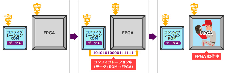
Simply put, it is loading design data into an SRAM-based FPGA.
FPGAs are SRAM-based devices, so nothing happens when you turn them on. To work, the FPGA design data must be transferred from ROM.
This is called configuration.
Configuration after power-up is generally initiated automatically.
The FPGA design data (configuration data) must be written to the configuration ROM in advance.
This is called programming.
For programming, I will show you an example in another article.
Programming to EPCQ device via FPGA (JIC programming)
Configuration type (scheme)
There are three main types of configuration (schemes).
The state of the MSEL pin that determines the configuration mode is recognized at power-on, and configuration is performed according to that mode. The relationship between MSEL pin settings and configuration modes varies by FPGA family, so be sure to check the documentation for your FPGA.
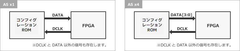
Active mode
The FPGA itself controls configuration and receives design data from the configuration ROM.
Configuration ROMs that can be used are Intel's genuine configuration devices (EPCQ-A / EPCQ / EPCS) and some third-party Flash memories.
Device Configuration - Support Center (Intel)
See also Design & Debug Guidelines.
Active Serial Configuration Design & Debug Guidelines
- Active Serial (x1): 1 line of data
- Active Serial (x4): 4 lines of data
Passive mode
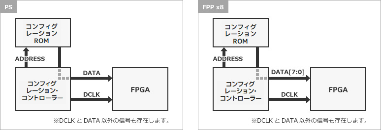
There is a device that controls the configuration externally, and the FPGA only receives design data from the configuration ROM.
Possible configuration controllers include MCUs and MAX® 10 / MAX® V / MAX® II with Parallel Flash Loader (PFL) IP. In the case of microcomputer control, the user must create all control programs. (Control by the free PFL IP is recommended because it is less burdensome for the user.)
Configuration ROMs that can be used are CFI / QSPI / NAND Flash memory.
- Passive Serial (PS)
1 DATA line received by FPGA (serial)
- Fast Passive Parallel (FPP)
Multiple DATA lines received by FPGA (8/16/32 lines)
When using PFL IP, the Flash memory supported by PFL is described in the user guide. See the documentation for details.
User Guide for Parallel Flash Loader (PFL) IP
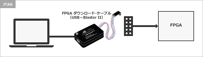
JTAG mode
JTAG mode is mainly used for debugging, and allows the SOF file to be configured directly from the FPGA's JTAG port using the Quartus® Prime Programmer using an Intel® FPGA download cable (USB-Blaster II, etc.).
How to choose the size of the configuration ROM
FPGA design data varies depending on the FPGA used. As a general rule, choose one that is larger than the RBF file size listed in your FPGA's documentation.
This configuration data can be compressed and stored in the configuration ROM. The compression rate at that time depends on the bitstream of the configuration data, so it is not possible to know the compression rate in advance.
Take the Cyclone® 10 LP as an example. The Cyclone® 10 LP is available in 8 Density (logic scale) devices as shown below, each with its own RBF size. Basically, use this RBF size as a guide when selecting the capacity for the configuration ROM. (When developing, be sure to check the latest English version of the document.)
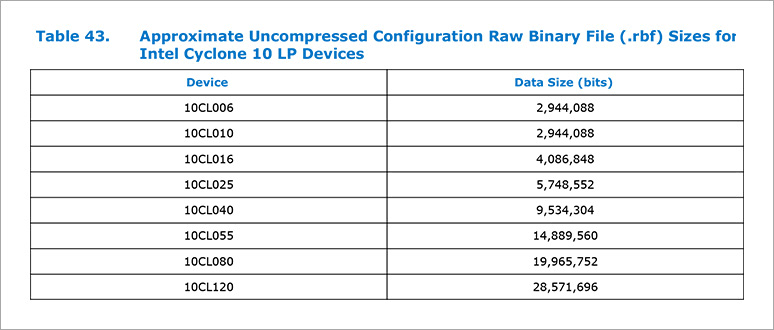
The configuration size for each FPGA can be found in the documentation.
Stratix® 10 / Stratix® V
Arria® 10 / Arria® V
Cyclone® 10 GX / Cyclone® 10 LP / Cyclone® V
* Search by keywords such as Configuration Bit Stream Sizes and Raw Binary File Size.
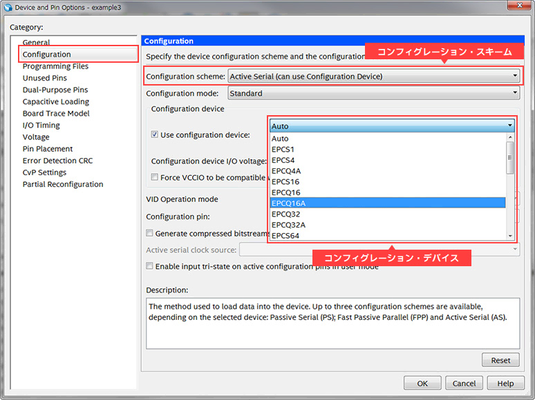
Configuration Settings in Quartus® Prime
If you set the configuration in Quartus® Prime, programming data will be generated automatically during compilation.
See here for configuration settings and conversion of programming data.
How to set Quartus® Prime device options
Generate or Convert Quartus® Prime Programming Files (Convert Programming Files)
Click here for recommended articles/materials
Active Serial Configuration Design & Debug Guidelines
How to set Quartus® Prime device options
Generate or Convert Quartus® Prime Programming Files (Convert Programming Files)
Intel FPGA Development Flow/FPGA Top Page
Click here for recommended FAQ
Click here for recommended seminars/workshops
Quartus® Prime Introductory Trial Course <Free>
Custom microcomputer design trial ~Experience embedded design using MAX® 10 FPGA! ~ <free>