- Semiconductor BusinessHOME
- Products and Services of Macnica,Inc.
-
technical information

-
Events and Seminars
- Handling Manufacturer
- Support
- Inquiry
- Click here to purchase products
- Semiconductor business e-mail magazine registration
![]()
![]() Narrow down by specifying conditions
Narrow down by specifying conditions
現在2184件がヒットしています。check
Last time, I talked about setting up simultaneous equations for the four constants of integration, A11, A12, A21, and A22. This time, I will explain how to solve the simultaneous equations and find the waveform.
The equation contains an exponential function with s for the Laplace transform. The Laplace transform used here is only the time delay. That is, if the Laplace transform of the time function f(t) is F(s), the inverse Laplace transform of F(s)×exp(-sτ) is f(t-τ), that is, the time delay.
system of equations for constants of integration
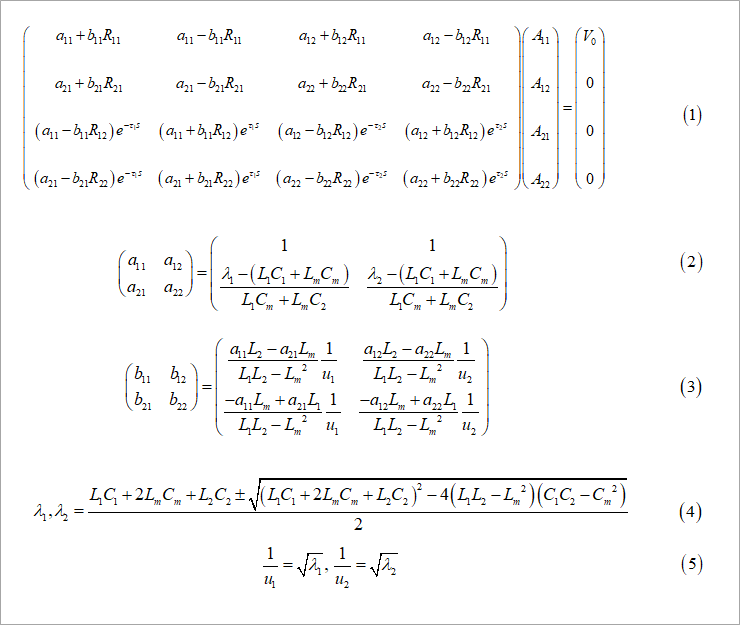
Equation (1) in Figure 1 shows the simultaneous equations for the constants of integration A11 to A22.
The aij and bij matrices are the same as mentioned last time. This is also reproduced in equations (2) and (3).
Please refer to the previous column for λ1, λ2, etc. in formulas (4) and (5).
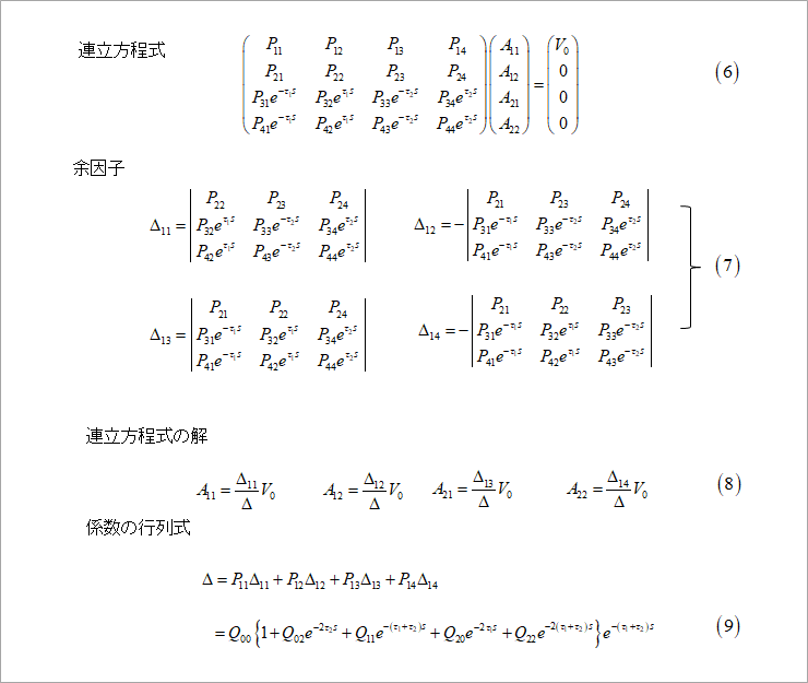
Since the coefficients of the simultaneous equations are complicated, they are displayed as Pij as shown in Equation (6) in Figure 2. The matrix on the left side of the left side is the coefficient, the next column matrix is the unknowns A11 to A22, and the right side is the constant term. For simultaneous equations, up to three unknowns (ternary), the determinant of the coefficients is solved by the cross-multiplication (Sarrus) method. I have.
This equation is a little easier because the right hand side (constant term) is only the first row and the others are 0s. We need only four cofactors for the first row of the matrix of coefficients, namely Δ11 to Δ14 shown in equation (7) in the same figure. Δ11 is the minor determinant of the coefficient's determinant as seen from row 1, ie, excluding the first row and first column. Due to the nature of the determinant, Δij is signed as (-1)^(i+J). That is, the signs of Δ12 and Δ14 are negative. The unknowns A11 to A22 are obtained as shown in equation (8) in the same figure.
Here, Δ in equation (9) is the determinant of the coefficients of the above equation, arranged by the exponent of the combination of times τ1 and τ2.
Series expansion of fractions
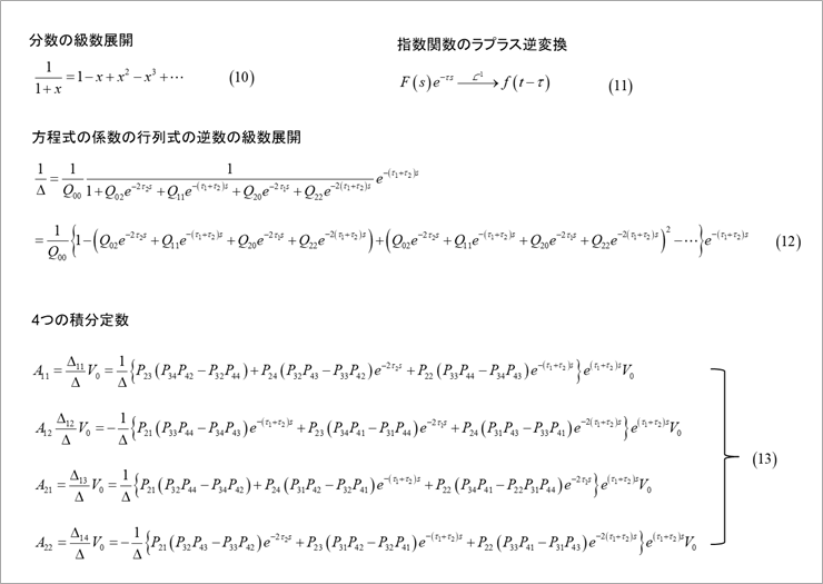
Δ in Equation (9) in Figure 2 is the denominator of Equation (8), and is series-expanded according to Equation (10) in Figure 3. Also, exp(-τs) becomes a time delay when inversely transformed into Laplace, as shown in equation (11). Based on equation (10), equation (9) is expanded as equation (12).
The series expansion of this denominator is quite complicated and requires patience to solve. The x in the denominator of equation (10) contains four terms, as can be seen from equation (9). Squaring this gives us 4 x 4, or 16 terms. Considering up to 3 round trips of the signal, 3 to the 3rd power of 4 is 64 terms, and 4 round trips is 256 terms to the 4th power, which is a huge amount of calculation.
However, since the same timing data appears in the 16 terms of the square, there are actually 9 terms. Multiplying this 9 terms by 4 terms of x gives 36 terms, and if this is also combined at the same timing, it will be 15 terms. Furthermore, substituting equation (12) into each equation of equation (8), we get equation (13). Usually, the crosstalk calculation will be somehow practical with two round trips.
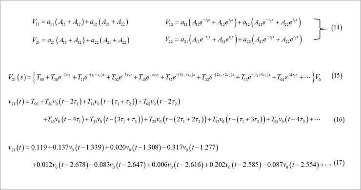
Using A11 to A22 obtained from equation (13), the near-end and far-end voltages are obtained from equation (14) in Figure 4. a11 to a22 in the same formula are formula (2) in Fig. 1.
Equation (14) is summarized for each exponent as in Equation (15).
The inverse Laplace transform of Equation (15) is expressed as the sum of the time delays of the signal sources multiplied by coefficients, as shown in Equation (16).
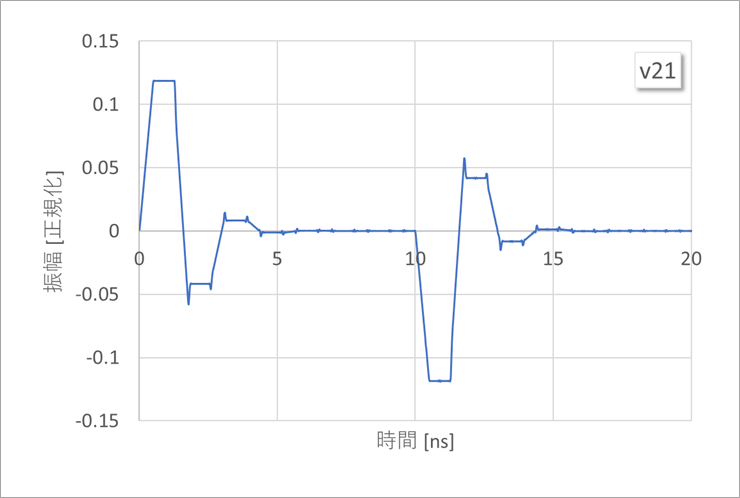
Equation (17) is the result of calculating v21 for the circuit in Figure 5. Up to 2 round trips (4τ) are described here.
The above calculations assume a surface layer (microstrip line) with different delay times for the two modes. For an intermediate layer (stripline) where the delay times of the two modes are equal, Equation (12) simplifies considerably, facilitating series expansion.
Analysis example
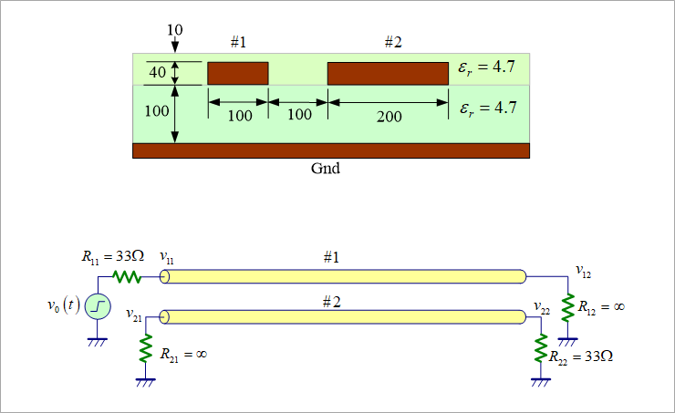
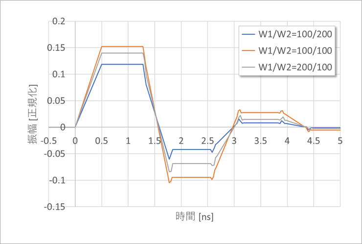
Figure 5 shows the circuit for analysis. Line #1 and line #2 are asymmetric lines with pattern widths of 100um and 200um, respectively.
Find the near-end crosstalk v21 where line #1 is the aggressor line and line #2 is the victim line, and the directions of the signals on both lines are opposite.
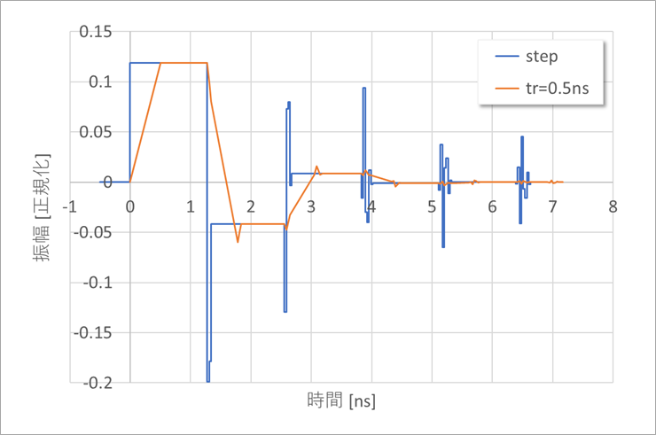
The terms of equation (17) in Figure 4 are illustrated in Figure 6(a). Here, v0(t) of the signal source is a step waveform.
Figure 6(b) adds those terms together, which is v21 or near-end crosstalk.
The figure looks different from the actual crosstalk. This is because the rising edge of the signal is a step waveform with 0 (zero).
Since this example is a surface layer (microstrip line), whisker-like noise occurs due to the difference in delay time between the two modes, but this whisker does not occur in the middle layer (strip line).
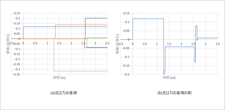
Figure 7 shows the sum of (a) terms and (b) terms for a finite rise time, tr = 0.5ns, as in Figure 6.
It can be seen that the steep narrow pulse width in Figure 6 is buried in the rise time.
Compare Figures 6 and 7 to understand how the whiskered pulse is generated and actually hidden.
Around 1.3 ns in one round trip of the line, a combination of two modes of delay time, that is, 2τ1 = 1.339 ns, τ1 + τ2 = 1.308 ns, 2τ2 = 1.277. It is
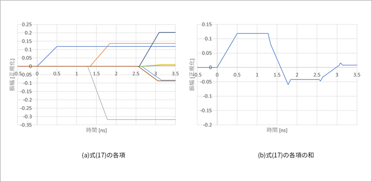
Figure 8 compares a step waveform and v21 with a finite rise, tr=0.5ns.
Waveforms at each part of the near end and far end
Figure 9 shows the waveforms for the near and far ends except for v21.
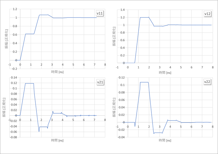
Figure 10 shows a comparison of V21 when W1 and W2 are varied.
Fourier transform method
Setting the s of the Laplace operator in formula (1) in Fig. 1 to jω and setting the period will result in a Fourier transform.
For the Fourier transform, see below.
Laplace transform and Fourier transform
https://www.macnica.co.jp/business/semiconductor/articles/basic/128001
FFT by Excel
https://www.macnica.co.jp/business/semiconductor/articles/basic/128345
FFT by Excel (Part 2)
https://www.macnica.co.jp/business/semiconductor/articles/basic/134557
Equation (8) in Figure 2 is obtained, and the waveform is obtained by obtaining Equation (13), giving the signal source, and performing inverse Fourier transform without performing series expansion as in Equation (12) in Figure 3.
Figure 11 shows the analysis results of 4096-point FFT with a period of 100ns and a pulse width of 10ns.
The most difficult part of the Laplace transform method is the expansion of equation (12) in Figure 3.
The Laplace transform is basically the analysis of a single-shot phenomenon, and the Fourier transform assumes periodicity.
Figures 12 and 13 show examples of actual analysis, as using only formulas does not give you a sense of reality.
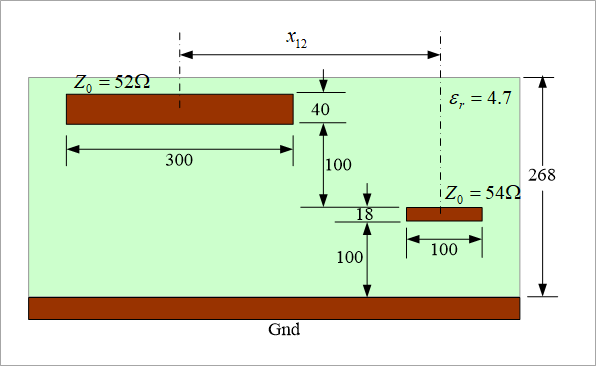
Figure 12 shows an example where L1 and L2 are above the ground plane of L3.
Since the distance between L1 and L3 is as large as 218um, the pattern width is 300um in order to make the characteristic impedance approximately 50Ω. L2 under it has a pattern width of 100um and a characteristic impedance of 54Ω.
Crosstalk between layers must be considered between L1 and L2.
CAD verification of layer-to-layer crosstalk is not very straightforward. (At least it was difficult in the past)
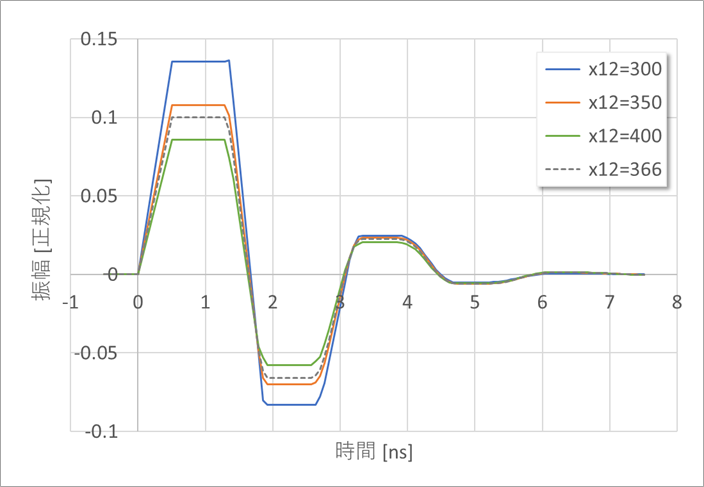
Figure 13 shows an example of analyzing the near-end crosstalk from L1 to L2 for the cross-section of Figure 12.
Analysis was performed by changing the center distance between patterns in Fig. 12 from 300 to 400um.
The center distance when the near-end crosstalk becomes 0.1 is 366um.
In this way, in the case of an asymmetrical line, there is no way to decompose it into the two modes of common and differential as in the case of a symmetrical line, so the calculation becomes quite complicated.
Next time, I plan to describe a slightly smarter solution using eigenvectors.
References
Yuzo Usui: All About Distributed Constant Circuits for Board Designers (3rd Edition) Self-published, 2016
What is Yuzo Usui's Specialist Column?
It is a series of columns that start from the basics, include themes that you can't hear anymore, themes for beginners, and also a slightly advanced level, all will be described in as easy-to-understand terms as possible.
Maybe there are other themes that interest you!