- Semiconductor BusinessHOME
- Products and Services of Macnica,Inc.
-
technical information

-
Events and Seminars
- Handling Manufacturer
- Support
- Inquiry
- Click here to purchase products
- Semiconductor business e-mail magazine registration
![]()
![]() Narrow down by specifying conditions
Narrow down by specifying conditions
現在2175件がヒットしています。check
Analysis of reflected waveform
The following methods have been described for the analysis of reflected waveforms.
■ Reflection analysis using IBIS - Part 1, Part 2
https://www.macnica.co.jp/business/semiconductor/articles/basic/111905
https://www.macnica.co.jp/business/semiconductor/articles/basic/112009
■ Bergeron chart
https://www.macnica.co.jp/business/semiconductor/articles/basic/122501
■ Nonlinear Bergeron chart
https://www.macnica.co.jp/business/semiconductor/articles/basic/122797
■ Grid diagram
https://www.macnica.co.jp/business/semiconductor/articles/intel/122061
Differential equation solution
Here, we will return to the origin, set up an equation from an equivalent circuit, and describe how to solve a differential equation.
I tend to shy away from formulas, but I'll go into a little bit of verbose detail, so don't be shy and read on. If you are good at formulas, I think you can understand it even if you read it a little diagonally.

Figure 1 is an equivalent circuit of a distributed constant circuit. As the name suggests, circuit constants are connected in a distributed manner. Circuit constants are capacitors and inductors.
See also
"Distributed constant circuit - what is distributed? 』
https://www.macnica.co.jp/business/semiconductor/articles/basic/110389
In addition, there is a leakage conductance G in parallel with the capacitor and a resistance R in series with the inductor, which we ignore here. In the figure, the capacitor is CΔx and the inductor is LΔx, but since C and L are values per unit length (meter), they are multiplied by the minute interval Δx. Think of Δx as a minute interval without defining a specific value. Same as dx of derivative d/dx.
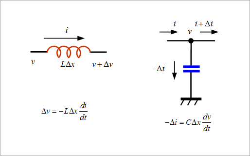
Figure 2 shows the relationship between voltage and current for inductors and capacitors. The inductor voltage drop is the product of the inductor and the derivative of the current. Since it is a voltage drop, it has a negative sign. The formula for the current in a capacitor is not very familiar, but it is the differentiation of both sides of charge = capacitor x voltage. The derivative of charge is the current. In other words, the integral of the current is the charge.

Figure 3 shows the process of transforming the inductor voltage and capacitor current equations in Figure 2 into a differential equation.
First, dividing both sides of equations (1) and (2) by Δx and making Δx infinitesimal gives the differentiation of equations (3) and (4). In addition, since there are two independent variables, the distance x and the time t, it is a partial derivative.
Differentiating both sides of equation (3) with respect to x gives equation (5).
The derivative of the current with respect to x on the right side of equation (5) is the same as equation (4), so substitute equation (4) to get equation (6).
Equation (6) is called the wave equation.
Apply the Laplace transform to equation (6).
The Laplace transform converts a differential equation into an arithmetic equation, just put s for d/dt. This allowed me to convert the partial differential equation to the ordinary differential equation (7).
Equation (7) is the simplest second-order linear differential equation.
The solution is given by equation (8), where A1 and A2 are the constants of integration.

Next, find the current in Figure 4.
Laplace transform the partial derivative of equation (3) to obtain equation (9) and find the current I in equation (10).
Differentiating equation (8) with respect to x gives equation (11).
By substituting dV/dx in equation (11) into equation (10) and successively transforming the equations, we obtain equation (12). Here, the characteristic impedance Z0 is defined as shown in Equation (13).
boundary condition
The two integral constants are determined from the near-end and far-end voltage-current relationships. Equation (14) in Figure 5 is the relationship between voltage and current at the near end, and Equation (15) is the condition at the far end.
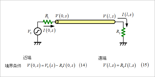
Figure 6 derives the equations for the two integration constants A1 and A2 from the near-end boundary conditions. First, substitute x=0 for each of V(x,s) and I(x,s) in Eq. (14) for the near-end boundary condition.
Voltage V is obtained by substituting x=0 into equation (8) to get equation (16).
For current I, substitute x=0 into equation (12) to obtain equation (17).
Equation (18), which is obtained by substituting Equations (16) and (17) into Equation (14), is rearranged for A1 and A2 to obtain Equation (19). Here is one of the simultaneous equations for A1 and A2.

Figure 7 derives another equation for A1 and A2 from the far-end boundary conditions as well as the near-end. Substitute x=l(el) for each of V(x,s) and I(x,s) in equation (15) for the far-end boundary condition.
The voltage V is given by equation (20) by substituting x=l into equation (8).
Current I is obtained by substituting x=l into equation (12) to get equation (21).
where √LC×l is the delay time τ of the signal from near-end to far-end. Formula (22), which is obtained by substituting formulas (20) and (21) into formula (15), is rearranged for A1 and A2 to obtain formula (23). Here is another one of the system of equations for A1 and A2.

Equations (19) and (23) in Fig. 8 are simultaneous equations for A1 and A2. Since it is a binary (two unknowns) system of equations, it should be easy to solve.
It may be easier, especially numerically, to put it in matrix form and solve it using Sarrus' method.
Equation (24) is a matrix form of equations (19) and (23).
Equation (25) is the determinant Δ of the coefficients of Equation (24).
Equations (26) and (27) are the solutions of this simultaneous equation.

Figure 9 rearranges equations (26) and (27) and rewrites them as equations (28) and (29). where Equations (30) and (31) are the reflection coefficients at the near and far ends, respectively.
For the reflection coefficient,
"Reflection coefficient"
https://www.macnica.co.jp/business/semiconductor/articles/basic/132300
Please refer to
Substituting equations (28) and (29) into the far-end voltage, equation (20), we get equation (32).
Equation (32) is a Laplace-transformed formula, so if you inverse Laplace-transform it, it becomes a time function.
For the Laplace transform,
"Laplace transform and Fourier transform"
https://www.macnica.co.jp/business/semiconductor/articles/basic/128001
See also

Figure 10 reproduces the Laplace transform formula from Figure 2 of the article above.

Equation (32) in Figure 9 has no conversion formula in the formula in Figure 10. The fraction in equation (32) can be expanded into a series as shown in equation (33) in Figure 11. The formula for the sum of infinite geometric series. Therefore, by rewriting equation (32), we obtain equation (34). Inside { } in the same equation is the top conversion (time delay) on the right side of Fig. 10, equation (35).
Using this formula, the inverse Laplace transform of equation (34) yields equation (36). The output waveforms of the drivers delayed by odd multiples of τ are sequentially multiplied by the reflection coefficient r1r2 and added.

Figure 12 shows an example of the calculation result of equation (36). To exaggerate the reflection, I set R1=11Ω (equivalent to a 24mA driver) and τ=0.35ns (about 5cm). The step waveform has a rise time of zero, and the ramp waveform has a rise time of 0.5 ns (0%-100%). The waveforms of τ, 3τ, 5τ, etc. multiplied by the reflection coefficient r1r2 are shown on the left of the figure, and their addition on the time axis is shown on the right of the figure.

Figure 13 shows the calculation results for a rise time of 1 ns. From the magnitude relationship between the rise time tr and the round-trip time 2τ, we can see that the reflected waveform has not reached its full amplitude. Compare with Figure 12.

appendix
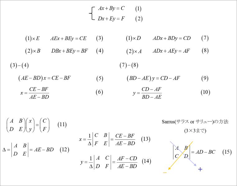
Review how to solve simultaneous equations with two variables (binary).
The unknowns in equations (1) and (2) solve a system of equations for x and y. First, to eliminate y, multiply both sides of equation (1) by E and both sides of equation (2) by B to get equations (3) and (4). Subtracting both sides of equations (3) and (4) eliminates the y term, resulting in equation (5), from which x can be found as in equation (6).
Similarly, multiplying formula (1) by D, and multiplying formula (2) by A and subtracting each side yields formula (9), which gives y in formula (10). Now that we've reached our goal, I'll show you how to use determinants. Express the simultaneous equations of equations (1) and (2) in a matrix as shown in equation (11). Equation (12) is the determinant Δ of the coefficients of Equation (11). x is obtained by replacing the first column of equation (11) with the matrix on the right side, calculating the determinant, and dividing by the determinant of the coefficients Δ. Similarly for y, replace the second column of equation (11) with the matrix on the right side, find the determinant, and divide by Δ. Up to 3×3, the determinant is calculated by Sarrus's method (cross-multiplication operation) in formula (15), with the downward-sloping multiplication being positive and the left-sloping multiplication being negative.
What is Yuzo Usui's Specialist Column?
It is a series of columns that start from the basics, include themes that you can't hear anymore, themes for beginners, and also a slightly advanced level, all will be described in as easy-to-understand terms as possible.
Maybe there are other themes that interest you!