- Semiconductor BusinessHOME
- Products and Services of Macnica,Inc.
-
technical information

-
Events and Seminars
- Handling Manufacturer
- Support
- Inquiry
- Click here to purchase products
- Semiconductor business e-mail magazine registration
![]()
![]() Narrow down by specifying conditions
Narrow down by specifying conditions
現在2004件がヒットしています。check

Measurement of characteristic impedance
The characteristic impedance of the board traces is usually measured by the TRD (Time Domain Reflectmety) method.
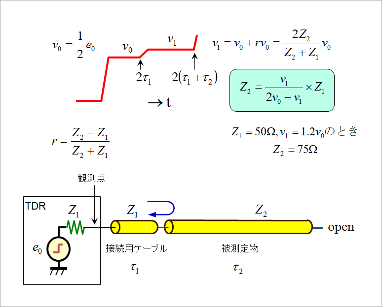
Figure 1 is the equivalent circuit for that measurement. From the TDR main unit, an extremely fast pulse waveform with a rise time of several tens of ps or less is sent out. If you just want to measure the characteristic impedance of a line, you don't need such a fast start-up. of pulses is required.
TDR measurement principle
The output impedance of the TDR is Z1 (usually 50Ω), and the TDR and device under test (DUT) are connected with a cable with a characteristic impedance of Z1 (50Ω). This cable can usually be regarded as an ideal cable with negligible loss, so no reflection occurs at the connection point with the output impedance of the TDR. The reflection coefficient at the connection point between the cable (characteristic impedance Z1) and the DUT (characteristic impedance Z2) is r=(Z2-Z1)/(Z2+Z1). (Please refer to the trivia "Reflection Coefficient".)
It is difficult to see the formula below, so only the formula is shown in Fig. 2. Please take a look and compare with the text.
The voltage v1 at the connection point between the cable and the DUT is given by the incident wave v0:
v1=v0+rv0=2Z2/(Z2+Z1)v0
and Z2 is obtained from this formula,
Z2=v1/(2v0-v1)×Z1=v1/v0/(2-v1/v0)×Z1
becomes.
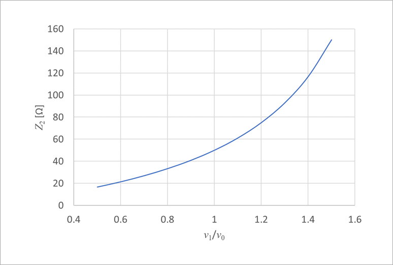
Figure 3 shows the DUT characteristic impedance Z2 with respect to v1/v0, where Z1=50. In other words, it indicates that the characteristic impedance can be read at the amplitude of the first rise. The TDR is actually set up so that Z2 can be read directly from this calculated scale.
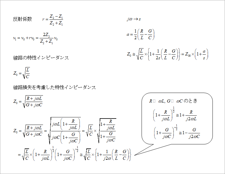
Equation of characteristic impedance and line loss
The characteristic impedance Z0 of the line is expressed as Z0=√(L/C) by the line inductor L (H/m) and capacitor C (F/m). (Please refer to "Distributed constant circuit - what is distributed?")
Actual lines have losses due to resistive loss and dielectric loss. (See "Line Loss and Waveform".)
These line losses are a function of frequency and are difficult to analyze with a simple SPICE like PSPICE. Generally, HyperLynx or W element of HSPICE is used. The author solves it on the frequency axis and converts it to the time axis with FFT to obtain the waveform. The characteristic impedance considering the line loss is
Z0=√{(R+jωL)/(G+jωC)}
is represented by For example, an example of the line constant for a line with a differential impedance of 85Ω at 1GHz is
L-Lm=315nH/m → ω(L-Lm)=1979
C-Cm=150pF/m →ω(C-Cm)=0.942
R=58Ω
tanδ=0.02 → G=0.02
is.
Rewrite the expression for Z0 taking into account that R≪ωL, G≪ωC.
Z0=√(L/C)×√{(1+R/jωL)/(1+G/jωC)}
≒√(L/C)×{1+(R/LG/C)/(j2ω)}
To obtain the time response, using the Laplace transform s and setting jω→s in the above equation, we get
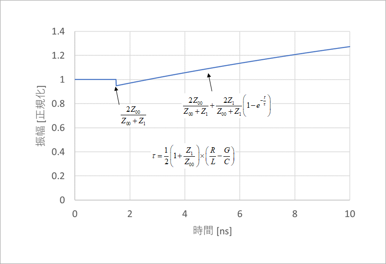
Z0≒√(L/C)×{1+(R/LG/C)/2s}=Z00×(1+a/s)
becomes. A variant of the equation below is shown in Figure 4. Here,
Z00=√(L/C)
a=(R/LG/C)/2
will do.
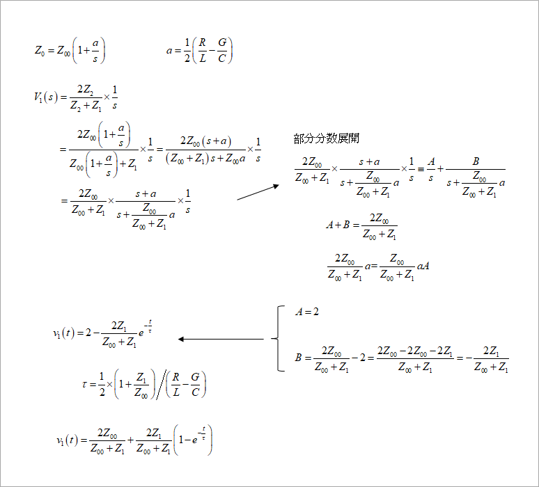
Time response by Laplace transform
Substitute this Z0 into Z2 in the equation for v1 to find the step response. Since the Laplace transform of the step waveform is 1/s,
V1(s)=2Z2/(Z2+Z1)/s
Since the transformation after this is complicated, it is summarized in Fig. 4. Expanding the above equation into partial fractions and inverse Laplace transform yields
v1 is 2-2Z1/(Z00+Z1)exp(-t/τ)
and converges to 2 at t=∞. Rewriting the above formula,
v1=2Z00/(Z00+Z1)+2Z1/(Z00+Z1){1-exp(-t/τ)}
Figure 5 shows an example of the calculation. In the example above, we set G=0. τ will be around 23ns.
Waveform of TDR
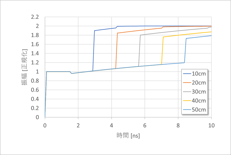
In practice, the reflection from the far end returns in a fairly short time, and the line length of the DUT interrupts this exponential waveform. becomes.
The author uses a PSPICE called MicroCap, and Fig. 6 shows the results of its analysis waveforms. This SPICE cannot handle dielectric loss, so only ohmic loss is given. Also, the frequency dependence of this ohmic loss is not reflected.
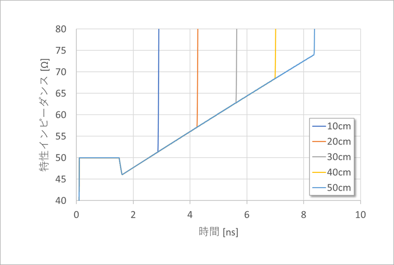
Figure 7 shows the value of v1 converted to characteristic impedance. A characteristic similar to that shown in Fig. 7 in "Substrate Characteristic Impedance Control" was obtained. Actually, it is necessary to reflect the frequency characteristics (skin effect) and dielectric loss of the resistor, but I think you can understand that the TDR waveform has a slope.
Note that the slope of the waveform is exaggerated because the resistance is the skin resistance at 1 GHz. To obtain the actual characteristics, as mentioned above, software that can analyze the frequency dependence of R and G and calculation using FFT are required.
References
Yuzo Usui : All about Distributed Constant Circuits for Board Designers (3rd edition) Self-published (http://home.wondernet.ne.jp/~usuiy/), pp. 171-180, 2016
What is Yuzo Usui's Specialist Column?
It is a series of columns that start from the basics, include themes that you can't hear anymore, themes for beginners, and also a slightly advanced level, all will be described in as easy-to-understand terms as possible.
Maybe there are other themes that interest you!