- Semiconductor BusinessHOME
- Products and Services of Macnica,Inc.
-
technical information

-
Events and Seminars
- Handling Manufacturer
- Support
- Inquiry
- Click here to purchase products
- Semiconductor business e-mail magazine registration
![]()
![]() Narrow down by specifying conditions
Narrow down by specifying conditions
現在2168件がヒットしています。check

Many people may find it difficult to adjust the phase compensation circuit in the circuit design of the DC/DC converter. If you can adjust it well, you can suppress the oscillation of the regulator and the large fluctuation of the output voltage in response to the fluctuation of the load connected to the regulator output.
However, if the adjustment of the phase compensation circuit fails and the phase margin is lost, a large ringing will occur in the output of the regulator or, in the worst case, it will oscillate (reference: phase margin measurement service).
There is a trade-off between regulator output oscillation and output fluctuations due to load fluctuations. This time, I tried to verify how much the load response characteristics are affected when the phase margin is set to an arbitrary condition (70°, 60°, 50° level) by adjusting the phase compensation circuit, which is a little troublesome. rice field.
Evaluation environment
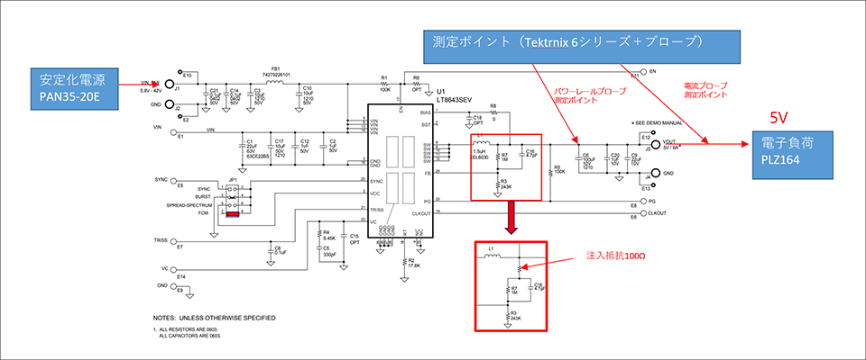
This time, we used the LT8643S evaluation board (DC2658A), which is a 42V withstand voltage synchronous rectifier MOSFET built-in step-down DCDC from Analog Devices.
Evaluation board settings
There are no changes from the original evaluation board other than adding a 100Ω signal injection resistor above the feedback resistor R7.
Evaluation conditions: Input voltage 8V / 12V / 16V (3 conditions), Output voltage 5V, Load current 1A / 3A / 6A (3 conditions) Switching frequency 2MHz setting
Measurement environment
- Stabilized power supply KIKUSUI PAN35-20E is used. Connect between VIN and GND on the evaluation board
・Uses electronic load KIKUSUI PLZ164WS. Connect between VOUT and GND
・Oscilloscope Tektronix 6 series is used. Ripple observed across output capacitor C6
- With Power Rail Probe TPR1000.
- Accessory 1.3m, SMA(Ma) - MMCX (Ma) , 50Ω cable
- Accessory MMCX connector (Wurth Elektoronik 66012002111503)
Verification of phase margin and load response characteristics
Evaluation board characteristics check
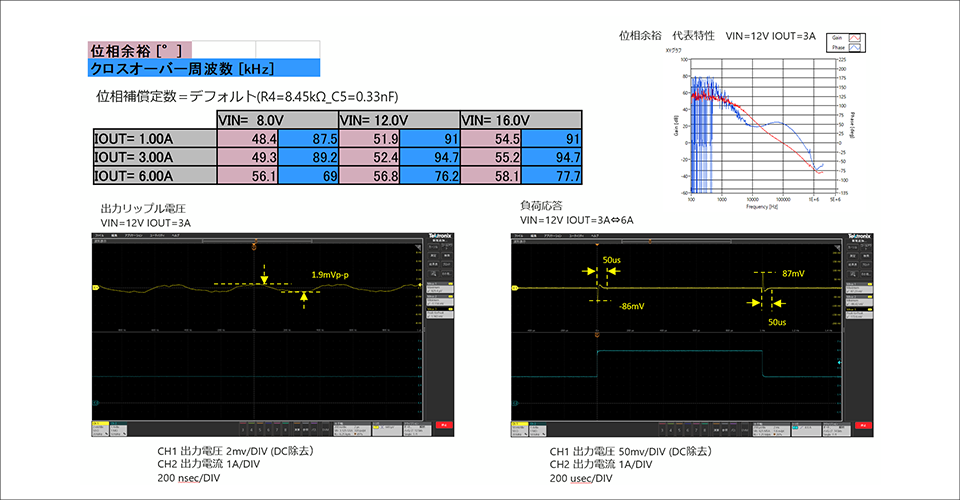
We checked the characteristics of the evaluation board in its initial state. The phase margin was 48.4 to 58.1°, and when checking the load response characteristics, the voltage fluctuation was ±87mV (crossover frequency 94.7KHz). The ripple voltage is a very small value of 1.9mVp-p.
As a power supply circuit, it has very good characteristics. From this state, I would like to verify how the load response characteristics change when the phase margin is changed.
When adjusted to the optimum phase margin
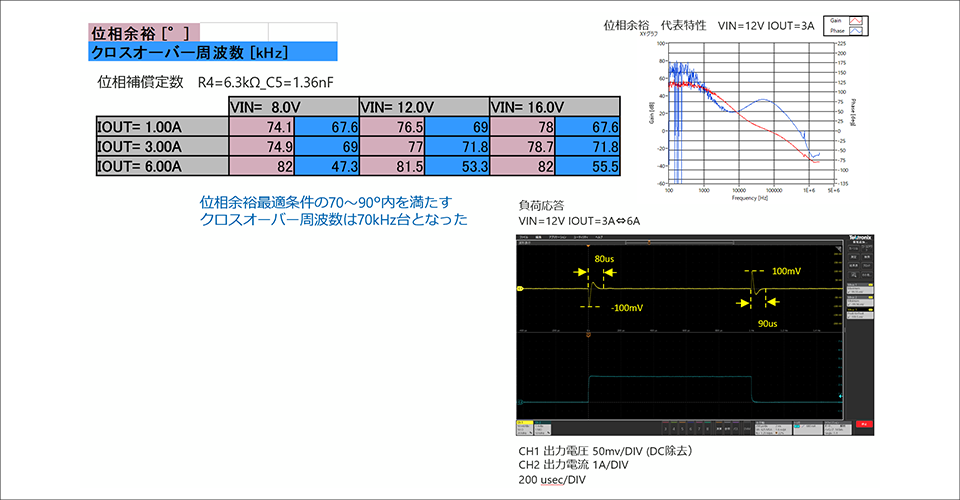
Fig. 3 shows the result of changing the constants to the optimum phase margin state by setting the phase compensation circuit to R4 = 6.3KΩ and C5 = 1.36nF.
The phase margin was 74.1 to 82°, and the voltage fluctuation was ±100mV (crossover frequency 71.8KHz) when checking the load response characteristics.
Improve load response characteristics by reducing phase margin
There is a trade-off relationship between phase margin and load response characteristics. In situations where it is necessary to improve the load response characteristics due to the requirements of the FPGA or CPU, it is necessary to increase the crossover frequency and improve the load response characteristics even if the phase margin is sacrificed to some extent.
Here, we changed the constants of the phase compensation circuit so that the phase margin becomes smaller, and checked whether the load response characteristics improved.
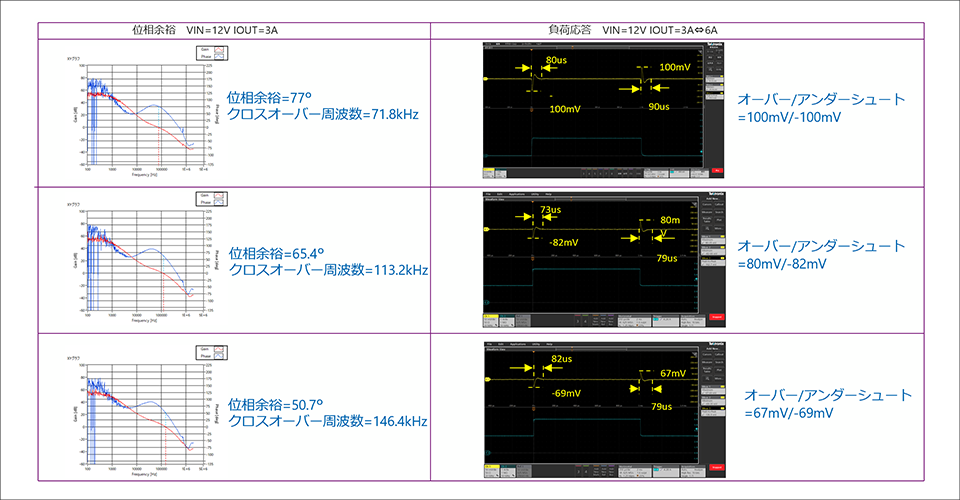
As shown in Fig. 4, reducing the phase margin increases the crossover frequency and improves the load response characteristics.
By improving the crossover frequency, we were able to suppress the voltage change to ±70mV (±1.4%) for an output of 5V.
From this, I hope you have understood that if you want to improve load response characteristics, it is important to increase the crossover frequency at the expense of the phase margin. However, please note that it is necessary to secure a phase margin of 45° or more.
Click here for recommended seminars/workshops
Click here for recommended articles/materials
LTspice List of articles: Let's use LTspice series
FAQ about power ICs: FAQ list
List of technical articles: technical articles
Manufacturer introduction page: Analog Devices, Inc.
Click here to purchase products
Click here for manufacturer site/other related links
Inquiry
If you have any questions regarding this product, please contact us using the form below.
Analog Devices Manufacturer Information Top
Analog Devices Manufacturer Information If you would like to return to the top page, please click below.