- Semiconductor BusinessHOME
- Products and Services of Macnica,Inc.
-
technical information

-
Events and Seminars
- Handling Manufacturer
- Support
- Inquiry
- Click here to purchase products
- Semiconductor business e-mail magazine registration
![]()
![]() Narrow down by specifying conditions
Narrow down by specifying conditions
現在2183件がヒットしています。check

How to suppress EMI?
In automotive applications, power supply EMI reduction is one of the key issues. It is important to minimize EMI generation factors in order to comply with the AM interference of power supply switching noise and the automotive EMI standard CISPR25 Class 5.
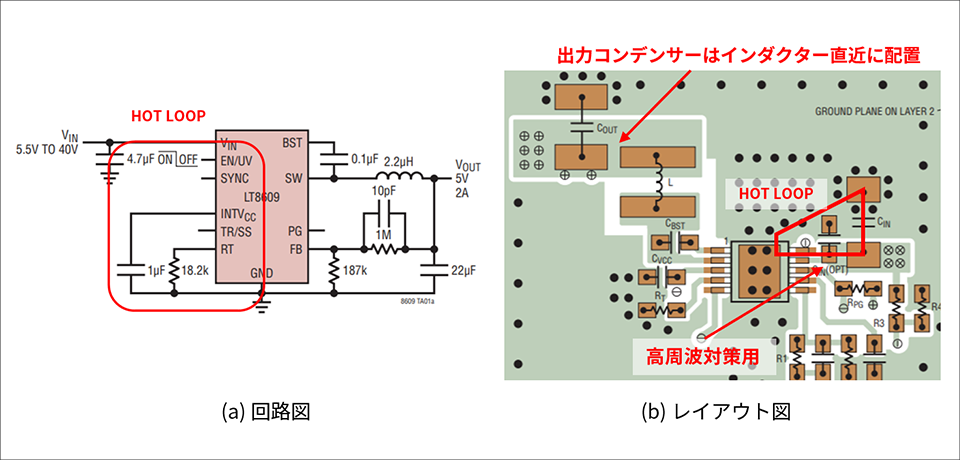
In a typical step-down switching regulator, the high di/dt current flow zone, the hot loop (shown in green in Figure 1), is the most EMI contributor. If we could reduce the board area of the hot loop to zero and obtain an ideal input capacitor with zero impedance, the effect of EMI would disappear, but on a real board, the effects of wiring and components cannot be eliminated.

Relationship between hot loop (high di/dt loop) and input capacitor
Let's consider EMI mitigation using the LT8609 as a reference. For internal FET types like the LT8609, the placement of the input capacitor in the hot loop is most important.
Input capacitors should be placed flush with the IC and close to the input pins of the IC to minimize hot loops. Also, in order to minimize parasitic inductance of wiring, it is necessary to connect with short and thick patterns. Placing the input capacitor on a different surface from the IC through vias will increase the hot loop length due to the inductance component of the vias, so be sure to place it on the same surface as the IC (Fig.2-(b)). For similar reasons, thermal relief should also not be used.
Using LTspice to check the effect of input capacitors
By using LTspice provided by Analog Devices, you can easily check the difference between when the input capacitor is properly placed near the IC and when it is not placed properly.
Figure 3 is the result of simulating the proper placement of the input capacitor.
I ran LTspice with no parasitic inductance between the input capacitor (C6) and the LT8609.
In the case of an ideal trace without pattern parasitic inductance, it can be confirmed that the input source V (input_power) and the voltage Vin near the IC are almost the same.
*In order to understand that there is a parasitic inductance between the input capacitor (C6) and the LT8609, a 3nH inductance is added to the input section just in case of abnormalities.
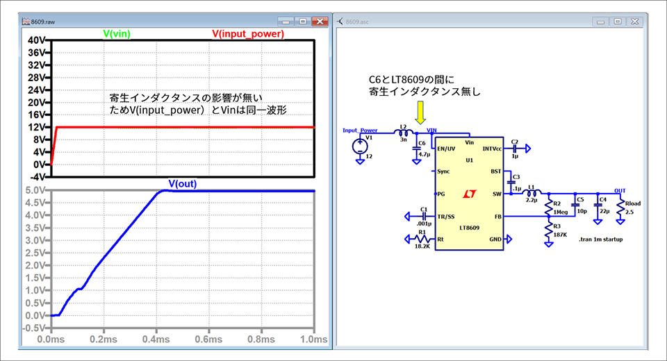
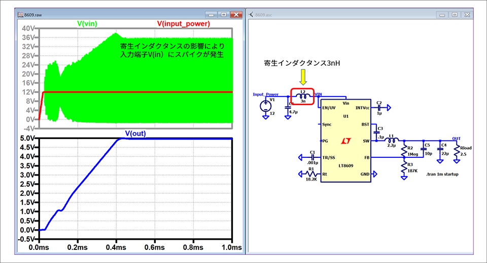
Figure 4 is a simulated result of a poor placement of the input capacitor.
Assuming that there is a wire with a width of 2 mm and a length of 6.5 mm between the input capacitor and the IC pin, 3 nH is placed as a parasitic inductance component.
By measuring the input voltage waveform V(in), we can see that voltage spikes can occur if the input capacitor is not properly placed.
As you can see from this result, it is important to properly place the input capacitor in the immediate vicinity of the IC.
Concerning frequency characteristics and arrangement of capacitors
input capacitor
Many switching regulators require a low capacitance on the input capacitor. ESR, ESLs of ceramic capacitors are used. Ceramic capacitors have frequency characteristics, and the smaller the capacitance, the higher the resonance frequency. EMI can be mitigated.
For the placement of the input capacitors for this combination, figure Please refer to 2-(b). Place a small high-frequency capacitor near the IC and a large low-frequency capacitor farther away.. In addition, ceramic capacitors have temperature characteristics, DC There are also points to be aware of, such as bias characteristics, so please carefully check the data sheet of each capacitor for details on component selection.
output capacitor
Unlike the input capacitor, a high di/dt current does not flow, but a ripple current flows in the output capacitor, generating a ripple voltage depending on the inductor current and the ESR of the output capacitor. The ripple voltage must be suppressed so that the output fluctuation including this ripple satisfies the design target.
As with the input capacitor, it is possible to minimize the ripple voltage by locating it close to the inductor to minimize the effect of pattern impedance and using a low ESR ceramic capacitor (Fig. 2). For details, please check the data sheet of each product.
Click here for recommended seminars/workshops
[Online Seminar] Analog Solution Power Supply Design Seminar <free>
[Online Seminar] Analog Solution Seminar Notes on Layout <Free>
[Online Seminar] Analog Solution Thermal Design Seminar <Free>
Inquiry
In this article, we introduced the importance of the position (capacitor type) of the DCDC input/output bypass capacitor used in automotive applications. For more information, please contact us below.
Analog Devices Manufacturer Information Top
If you want to return to Analog Devices Manufacturer Information Top, please click the button below.

![[Experiment report] Thumbnail image of video transmission evaluation when UTP cable is 100m or longer](/business/semiconductor/articles/Temp_ADI_Thumb_power_analog_15.png)