- Semiconductor BusinessHOME
- Products and Services of Macnica,Inc.
-
technical information

-
Events and Seminars
- Handling Manufacturer
- Support
- Inquiry
- Click here to purchase products
- Semiconductor business e-mail magazine registration


 Narrow down by specifying conditions
現在2237件がヒットしています。check

hello.
My name is Hanako Altera and I provide technical support for Altera® FPGA products at Macnica.
Altera®'s MAX® 10 is a non-volatile FPGA. It has built-in configuration flash memory (CFM), so no external configuration memory is required.
This time, we'll introduce a slightly unusual way to use CFM: "dual configuration."
Dual configuration overview
The MAX® 10 CMF can store up to two compressed configuration images and can switch between them during operation. This configuration is called a “dual configuration”.
(However, to store two images on the device, the compression ratio must be at least 30%.)
MAX® 10 has three types of function options: “Compact”, “Flash” and “Analog”.
Among them, only “Flash” and “Analog” which support “Dual Compressed Image” as configuration mode support dual configuration.
(However, since the flash type is not commonly used in WLCSP (Wafer Level Chip Scale Package), it can be said to be effectively "analog only".)
The MAX® 10 CFM consists of three sectors: CFM0/CFM1/CFM2. (10M02 is CFM0 only.)
CFM0 is used as the configuration image 0 region, and CFM1 and CFM2 are used as the configuration image 1 regions.

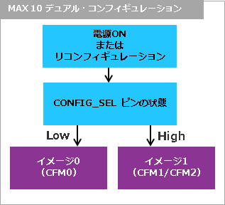
Dual configuration uses the MAX® 10 CONFIG_SEL pin for image selection. You can drive the CONFIG_SEL pin high or low externally to the device, and the state of this pin when the MAX® 10 powers up or starts reconfiguration determines which image is configured.
★ Reference material (From Device Pin Connection Guidelines)
"MAX 10 FPGA Device Family Pin Connection Guidelines"
let's prepare
To achieve dual configuration in MAX® 10, you need these:
● A development board with aMAX ® 10 device (with flash or analog feature options)
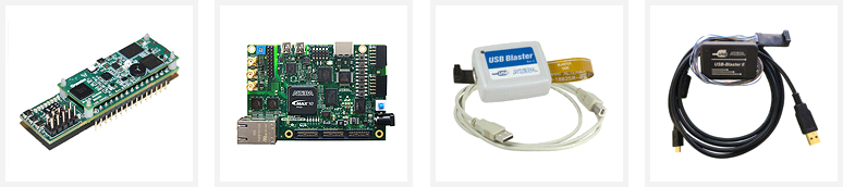
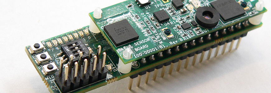
For example, you can use the Odyssey MAX® 10 FPGA Eva Kit (Odyssey) or the MAX® 10 FPGA Development Kit. (*As a board selection condition, it is an absolute requirement that the input to the CONFIG_SEL pin can be switched between High and Low.)
● Download cable corresponding to the development board being used
For the Odyssey, having a USB-Blaster™ or USB-Blaster™ II makes things much easier. (It's also possible to use a microUSB cable without one.)
The MAX® 10 FPGA Development Kit supports USB-Blaster™, USB-Blaster™ II, or Embedded USB-Blaster™ II via the included miniUSB cable.
● Quartus®Prime Lite Edition(Pro/Standard Editionis also acceptable)
MAX® 10 can be developed using free tools.
● Design project for the development board to be used
If you just want to get a feel for the workflow, try using the sample design for dual configuration! You can get the design project from the Design Store.
★ Reference article: Get free FPGA sample designs
Sample projects for dual configuration of the MAX® 10 FPGA Development Kit (for Quartus® Prime 16.0) are available here.
Let's try it
Rough work can be done by merging the SOF files of the two projects, but it is not enough to simply combine them. Include IP for dual configuration (available for free) in each project design.
The flow looks like this.
- Incorporating Dual Configuration IP into Your Design
- Option set for dual configuration support
- Compile to generate SOF
- Create POF file from SOF files of two projects
- Download POF to MAX® 10 device and check it works
- Check the operation by switching the input to CONFIG_SEL

1. Incorporate dual configuration IP into your design
Include IP for dual configuration at the top level of each project design.
First open one project and create the IP.
Launch Tools menu > Qsys, and double-click “Altera Dual Configuration” from the IP Catalog (upper left of the screen).
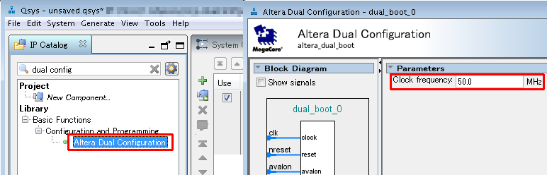
The parameter setting screen will be displayed, so set the frequency of the clock supplied to this IP. (For example, 50MHz for Odyssey and 4 clock frequencies for MAX® 10 FPGA development kit, so set the selected frequency.) Note that the maximum frequency that can be set is 80MHz.
Click the Finish button to have it added to your Qsys system.
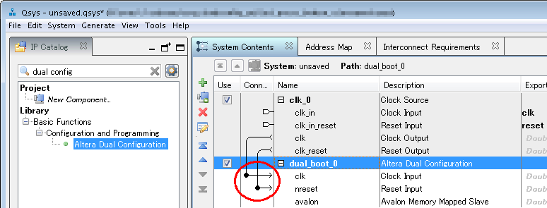
Connect the clock (clk) and reset (nreset) ports of the IP for dual configuration as shown below.
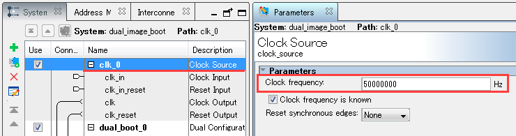
Set the clock frequency of Clock Source (default name clk_0) to the same value as the clock frequency of Altera Dual Configuration set earlier.
In Qsys File menu > Save As, specify the IP name and save folder.
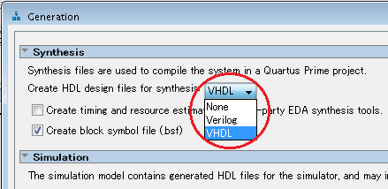
Click the Generate HDL button at the bottom right of the screen to display the Generation dialog Box. Specify the HDL language (Verilog/VHDL) to be generated for logic synthesis.
Check the Output Directory path and click the Generate button at the bottom right of the screen.
If you see a log in the Generate window and see the message “Generate: completed successfully”, IP creation is complete. Click the Close button and then the Finish button to close the screen.
A message will appear to add the .qip to the project. Select Add/Remove Files in Project (Project menu) and register the .qip file saved in the synthesis folder in the folder where the IP was generated using the Add button. increase.
Next, add the Altera Dual Configuration IP to the top level design of your project and connect the clock, reset (low active). Save your design after editing.
2. Option to support dual configuration
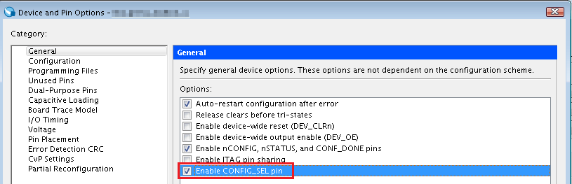
Set various options in Device and Pin Options (Assignments menu > Device).
[General category]
- Set the Enable CONFIG_SEL pin option = ON.
[Configuration category]
- Configuration Scheme: Internal Configuration
- Configuration Mode: Dual compressed images
- Generate compressed bitstreams オプション : ON
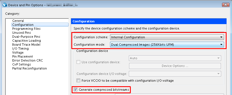
After setting, close all dialog Box with the OK button.
3. Compile to generate SOF
Double-click Compile Design in the Tasks window located at the bottom left of the Quartus® Prime screen to run and complete compilation. Then close the project.
* Do these steps 1 to 3 for the other project as well.
4. Create POF file from SOF files of two projects
Launch Quartus ® Prime File menu > Convert Programming Files and set the following.
[Output programming file]
- Programming file type: Programmer Object File (.pof)
- Mode: Internal Configuration
- File name: Specify the file name and storage folder of the POF file to be created (Set the Options/Boot info option as needed.)
[Input files to convert]
- Select SOF Data and click the Add File button. Select the SOF file of the project to write to CFM0 on Page_0.
- Click the Add Sof Page button to add Page_1. Select SOF Data at the bottom and click the Add File button. Select the SOF file of the project to write to CFM1 on Page_1.
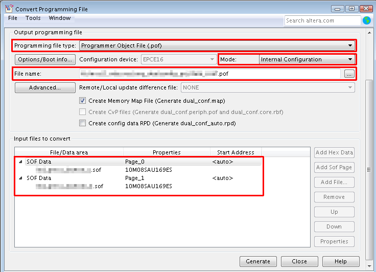
Click the Generate button and a POF file will be created with the message “Generated filename.pof successfully”.
Close the window with the Close button.
5. Download POF to MAX® 10 device and check operation
Before writing the POF file, check and set the status of the CONFIG_SEL pin.
By the way, in the case of Odyssey and MAX® 10 FPGA development kit, the CONFIG_SEL pin is designed to be pull-up/pull-down with a DIP switch.
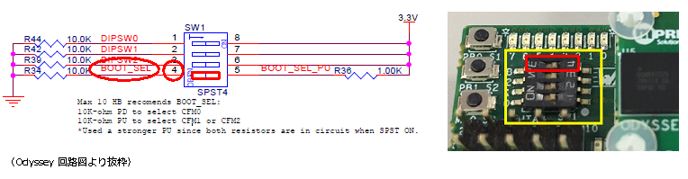
Now let's write the POF file to CFM in MAX® 10.
After preparing the board, download cable, etc., launch Tools menu > Programmer and set the following.
- Hardware setup: select download cable to use
- Mode: JTAG
- Add File button: select the created POF file
- Program/Configure オプション: ON
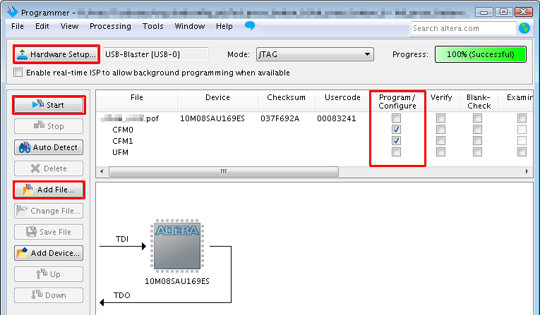
★ Reference information: If the USB-Blaster™ series name is not displayed in Hardware Setup...
Install the USB-Blaster™ driver
Install the USB-Blaster™ II driver
What to do if you can't install the USB-Blaster™ and USB-Blaster II drivers on Windows 10
Click the Start button to start writing!
Writing is complete when the Progress bar shows 100% and you can see the message “Successfully performed operation(s)” in the Messages window.
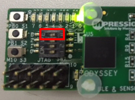
Power off the board and disconnect the download cable. Then turn on the power of the board again!
You can see that the CFM is selected according to the state of CONFIG_SEL on the board, and the image stored there is configured and working.
The image on the right shows the design in action with image 0 selected and LED0/LED1 alternately blinking.
(Sorry for the still image.)
6. Check the operation by switching the input to CONFIG_SEL
Next, let's switch the state of CONFIG_SEL.
Then power cycle the board (OFF→ON), or pull the nCONFIG pin low for more than a pulse width and then high again to reconfigure while the MAX® 10 is powered up.
The Odyssey has its nCONFIG pin pulled up (fixed) to 3.3V via a 10Ω resistor, so please turn it on again.
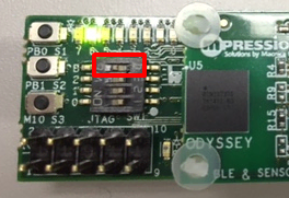
You can see that the other image is configured and working.
The image on the right shows the design in action with image 1 selected and LED6/LED7 alternately blinking.
(Sorry for the still image.)
The MAX® 10 FPGA development kit has a push button (PB) on the nCONFIG pin that pulses nCONFIG low to reconfigure without powering off the board. It is convenient because you can run
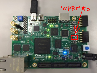
The MAX® 10 dual configuration system is now complete!
Everyone please come and experience it.
The development board and download cable that appeared this time can be purchased here, so you can experience it right away.
Related products