
![Isolated Gate Driver for Silicon MOSFET or SiC MOSFET NCP[NCV]51561](/business/semiconductor/manufacturers/142222_Onsemi_Product_cover.png)
Introduction
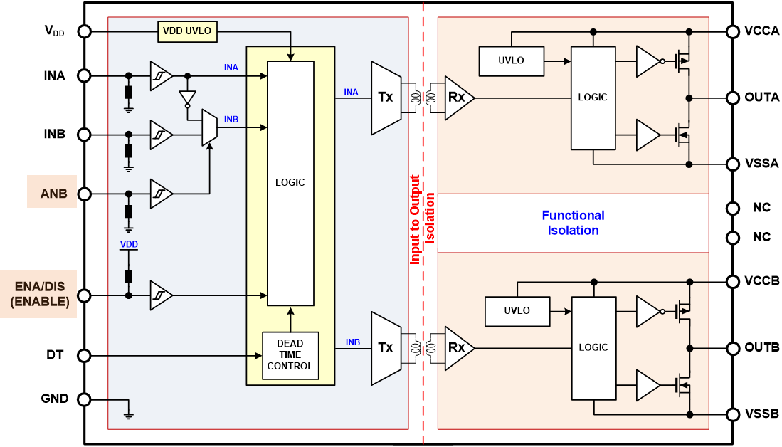
The NCP[NCV]51561 is an isolated dual-channel gate driver with source and sink peak currents of 4.5A/9A respectively. They are designed for fast switching to drive Silicon MOSFET and SiC MOSFET power switches.
Functions/features
・ 4.5A (sauce)/ 9A (sink) current
Supports dual low-side, dual high-side, or half-bridge gate driver control modes
・Independent for each output driver UVLO protection
・ CMTI(Common mode transient immunity)>200V/ns
・Propagation delay standard 36 ns
- maximum per channel 5 ns delayed matching of
-5 ns maximum pulse width distortion of
・Programmable input logic
-ANB Single or dual input mode with
-ENABLE or DISABLE mode
・Programmable dead time
・Insulation and safety standards
-5 kVRMS insulation (UL1577) and between output channels 1500V peak differential voltage
-8000 VPK Reinforced insulation voltage (VDE0884-11)
-GB4943.1-2011 according to CQC certification
-IEC 62386-1 based on SGS FIMO certification
・ NCV51561 is for automotive applications AEC-Q100 Correspondence
Main features
UVLO (low voltage malfunction prevention function)
It provides UVLO protection for VDD on the primary side and both gate driver outputs to VCCA and VCCB on the secondary side.
UVLO is 2.8Vtyp for primary side supply voltage 3~5V. Regarding the UVLO of the supply voltage for the gate driver output side of VCCA and VCCB on the secondary side, each voltage can be optionally selected as shown in Table 3 below.
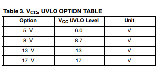
The optimum gate drive voltage value differs between driving a silicon MOSFET and driving a SiC MOSFET. You can select.
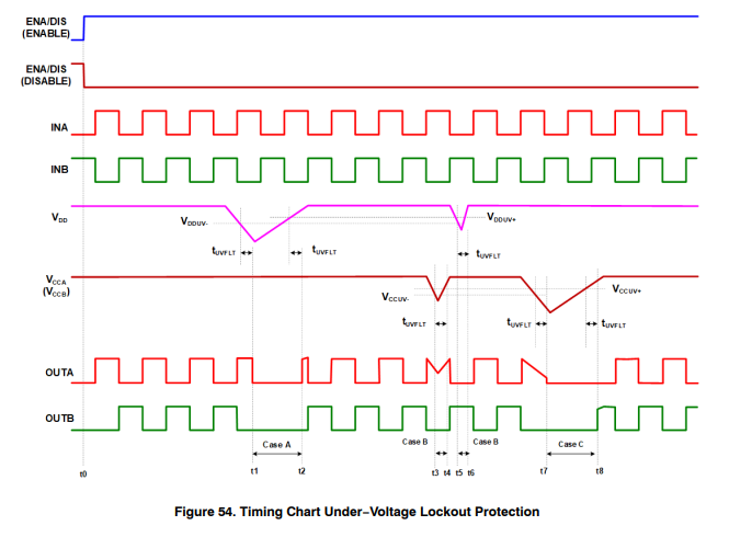
Fig.54 below shows the timing chart for UVLO protection.
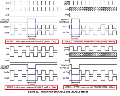
ENABLE or DISABLE mode
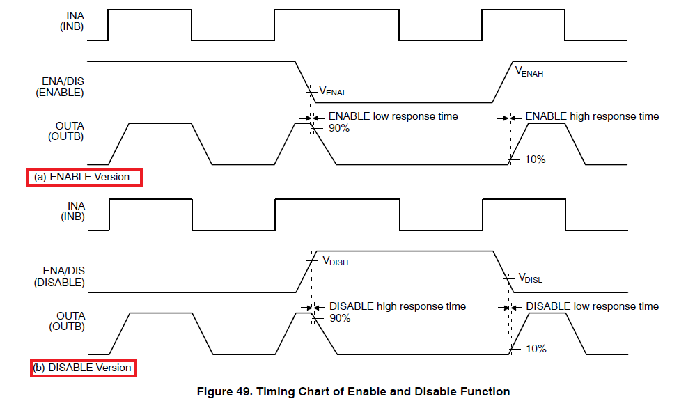
Fig. 49 shows the response time depending on ENABLE or DISABLE mode of operation.
As shown in the ENABLE version of Fig. 49(a), when the ENA/DIS(ENABLE) pin voltage goes to a LOW state, both outputs (OUTA&OUTB) are shut down simultaneously and the ENA/DIS(ENABLE) pin goes HIGH (or left open), it works fine in ENABLE mode.
Conversely, when the ENA/DIS(DISABLE) pin voltage goes to a HIGH state, both outputs (OUTA&OUTB) are shut down simultaneously and the ENA/DIS(DISABLE) pin is When pulled LOW (or left open), it works normally in DISABLE mode.
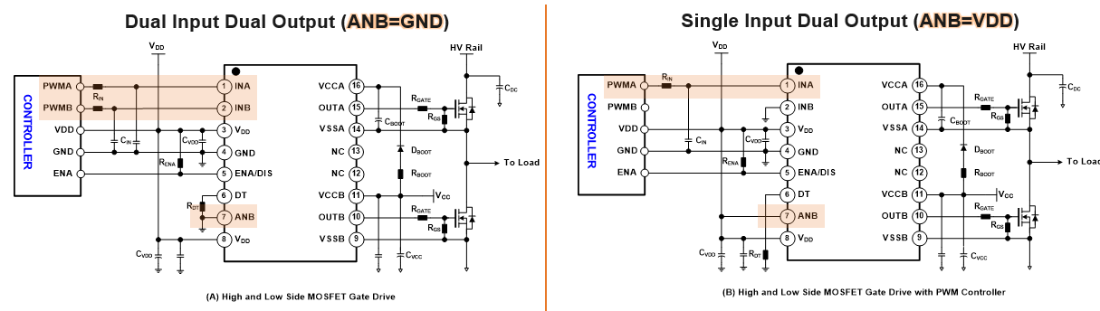
Dual input and single input
This product can set the input signal configuration with the ANB terminal.
As shown in the table below (Table.2), you can select the configuration from input channel to output channel (e.g. single input - dual output or dual input - dual output) and shutdown function (e.g. ENABLE or DISABLE). , which has four modes of operation.
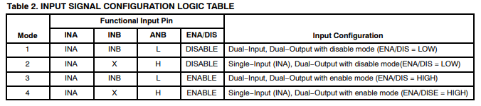
The figure below shows an example of ANB pin connection, and Fig.53 shows a timing chart of input/output and shutdown function by ANB pin and ENA/DIS pin.
programmable dead time
If the dead time between two external input signals (between the INA signal and the INB signal) is shorter than the internally set dead time (DT1 and DT2), the dead time is automatically inserted. Otherwise, if the dead time of the external input signal is greater than the internal dead time, the dead time is unchanged by the gate driver and internal dead time definitions, as shown in Fig.50.
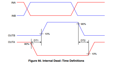
Deadtime monitors input timing and prevents output cross-conduction (such as a problem in a half-bridge configuration where both outputs are on at the same time).
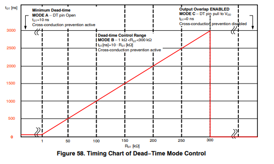
In dead time control, 3 There are two modes.
・ mode A: pin 6 (DT) floating.
20ns or less [Minimum dead time tDTMIN(typ)=10ns] dead time of , thus inhibiting cross-conduction of both channel outputs.
・ mode B: pin 6 (DT) the external resistor (1 kΩ ~ 300 kΩ) to adjust the dead time
tDT (in ns) = 10 x RDT (in kΩ)
・ mode C: pin 6 (DT) of VDD connect to
Cross-conduction protection for both channel outputs is disabled. (Non-half-bridge applications).
The figure below Fig.58 shows the timing chart of dead time control mode.
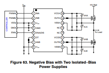
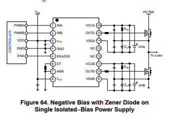
negative bias
When driving SiC MOSFETs, careful consideration is required to take full advantage of the operating characteristics of SiC. The gate driver must be able to supply +20 V and a negative bias of-2V to -5V. Parasitic inductance due to non-ideal PCB layout or long package leads can cause ringing in the power transistor's gate-source drive voltage during high di/dt and dv/dt switching.
There is even a risk of unintentional turn-on or shoot-through if the ringing exceeds the threshold voltage. Applying a negative bias to the gate drive is a common way to keep such ringing below threshold. A negative voltage can improve the noise immunity of SiC MOSFETs and suppress unintended turns. Figures 63 and 64 show examples of implementing a negative gate drive bias.
CMTI (Common Mode Transient Immunity)
The figure below shows the characteristics of CMTI.
Block Diagram
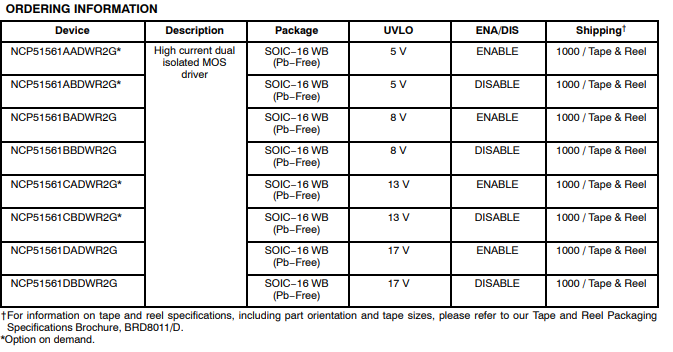
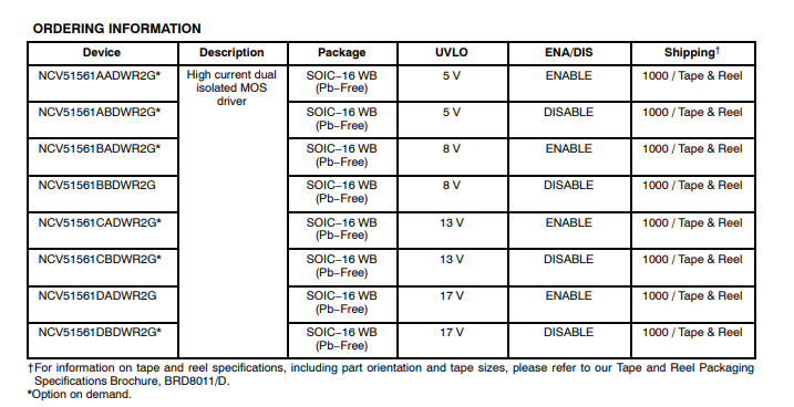
About the model number notation of the option selection part
NCP[NCV]51561 xy
・ UVLO value options (x): A: 5-V, B: 8-V, C: 13-V, D: 17-V
・ ENABLE/DISABLE option (y): A: ENABLE, B: DISABLE
-ENABLE version: Logic input high enables (ENABLE) both output channels. [Internal resistance pull-up]
-DISABLE version: A logic input high disables (DISABLE) both output channels. [Internal resistance pull-down]
Each model number information is shown below.
Evaluation Board
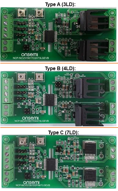
Several evaluation boards are available with different packages for the power devices to be driven. For details, please check the inquiry button or the Onsemi web page below.
https://www.onsemi.com/products/power-management/gate-drivers/ncp51561
lastly
If you would like to know more about this product, please check the data sheet on the ONSEMI website below.
Inquiry / Quotation
If you have any questions about this product or would like a quote, please contact us using the form below.
Onsemi Manufacturer information Top
If you want to go back to ONSEMI Manufacturer Information Top, please click below.