- Semiconductor BusinessHOME
- Products and Services of Macnica,Inc.
-
technical information

-
Events and Seminars
- Handling Manufacturer
- Support
- Inquiry
- Click here to purchase products
- Semiconductor business e-mail magazine registration
V-by-One® HS is a cutting-edge high-speed interface technology developed by THine Electronics, Inc. for the flat panel display market.
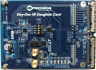
By connecting this daughter card to the HSMC connector of the Intel® FPGA development board on which the V-by-One® HS Tx/Rx IP is implemented, you can perform V-by-One® HS Interface verification work. increase. You can also verify not only the V-by-One® HS Tx/Rx IP, but also the FPGA built-in transceiver.
Verification of V-by-One® HS requires not only preparation of an Intel® FPGA development board, but also acquisition of Macnica V-by-One® HS Tx/Rx IP license (for evaluation or mass production) in advance Become.
The evaluation board that has been verified to connect with this card is the Intel® Cyclone IV GX FPGA Development Kit.
Specifications/Features
| model number | V BY ONE HS HSMC CARD |
| interface | HSMC, Hirose Electric FX16 connector |
| main parts | Si5317, IDT5V49EE504NLG, LT3029EDE |
| Others | Can be connected to an HSMC-equipped evaluation board Supports V-by-One HS up to 8 pairs Supports Macnica 's V-by-One HS IP |
Evaluation and verification example
If you use the included FFC cable, you can evaluate both Tx and Rx at the same time by loopback connection with just one set of development kit and card without preparing a separate kit for opposite connection.
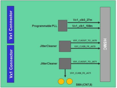
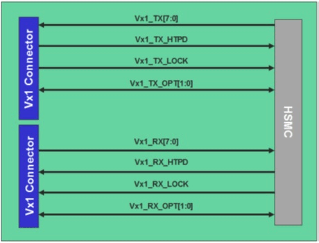
Block Diagram
V-by-One HS HSMC Daughter Card I/O Block Diagram
V-by-One HS HSMC Daughter Card Clock Block Diagram