- Semiconductor BusinessHOME
- Products and Services of Macnica,Inc.
-
technical information

-
Events and Seminars
- Handling Manufacturer
- Support
- Inquiry
- Click here to purchase products
- Semiconductor business e-mail magazine registration
![]()
![]() Narrow down by specifying conditions
Narrow down by specifying conditions
現在2004件がヒットしています。check
In the previous tutorial, we focused on the advantages of designing a power supply system composed of modules in terms of performance, design flexibility, and development speed, and in the second half, we confirmed the general flow of the design process. The modular approach is good, but requires external circuitry to turn the power distribution network (PDN) into a complete power system.
Part 2 of the tutorial addresses the first PDN challenge. Noise filters for the input and output sides of switching DC-DC modules.
Source of input noise
The switching operation of the DC-DC converter and the parasitic circuit elements distributed throughout the PDN generate two types of noise currents that should be filtered. Common mode noise and differential mode noise.
Common-mode noise originates from high-voltage switching nodes inside the converter and flows through parasitic capacitance to ground for EMI measurements. This noise comes out of both the positive and negative input terminals of the converter in phase and flows into the system ground. On the other hand, the switching operation of the converter produces differential mode noise, which flows only between the input terminals of the converter.
EMI Input Interference Problems and Solutions
These noises can cause many problems within the power system. The two DC-DC converters in Figure 2 interconnect not only the input DC power supply, but also the control and communication systems that are typically susceptible to noise. Noise generated by the DC-DC converter circulates throughout the PDN, causing unstable system operation and adversely affecting the operation of adjacent electrically connected systems.
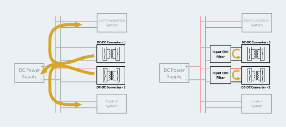
Figure 2: Noise from the converter propagates outside the module and can cause serious problems in control and communication systems.
When an input filter is added to the system, switching converter noise is bypassed so that it circulates only between the filter and the DC-DC converter, reducing interference with other systems connected to the same input power supply. This filter also works in the reverse direction to reduce the effects of external noise on the DC-DC converter.
When incorporating filters into power systems, depending on the application, compliance with EMC (Electromagnetic Compatibility) standards set by various international bodies is required. In addition, the standards can vary greatly depending on the industry and application. For example, standards differ significantly between defense applications and the automotive industry.
To reduce noise, several discrete components are used to effectively attenuate both common-mode and differential-mode noise currents. Common mode noise countermeasures generally use a common mode choke to increase the series impedance of the common mode circuit and attenuate the common mode current of the converter that flows out from the positive and negative input terminals. In order to feed common mode noise into the EMI ground, a Y capacitor is paired with a common mode choke to create a current path. (See Fig. 3)
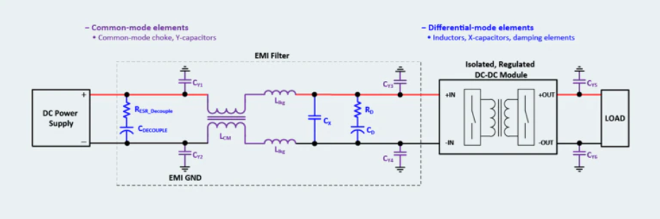
Figure 3: System with discrete common-mode and differential-mode noise filters
The element for attenuating differential mode noise is an inductor in series with the X capacitor. These elements create a high impedance current path for differential mode noise flowing out of the converter, creating a low impedance path that confines the noise current to the immediate vicinity of the converter.
If the signal ground and power ground are incorrectly connected when the noise current flows into the ground, the noise generated from the power components will flow into the control section. If the high-frequency noise generated by the DC-DC converter is coupled to the signal system by the parasitic capacitance of the wiring, it may affect the low-power control signal and cause unstable operation. To prevent power-related current from flowing through the signal ground, connect the signal ground to the power ground at only one point.
Filter topology
Although there are several filter configurations, this tutorial will focus on the most common second-order response filter. First, a simple inductor-capacitor filter characteristic has a second-order attenuation slope of –40 dB/dec above the cutoff frequency, as shown for the undamped LC filter in Figure 4. An undamped LC filter is generally not a good solution because it resonates at its corner frequency.
Without proper damping, this filter configuration will amplify noise near the resonance frequency. There are several methods for damping. First, it is a filter that adds a simple series damping by connecting a resistive element in parallel with an inductor. Although it has excellent corner frequency attenuation characteristics, it has the disadvantage of reducing the amount of attenuation in the high frequency region by adding a zero point to the frequency characteristics of the filter.
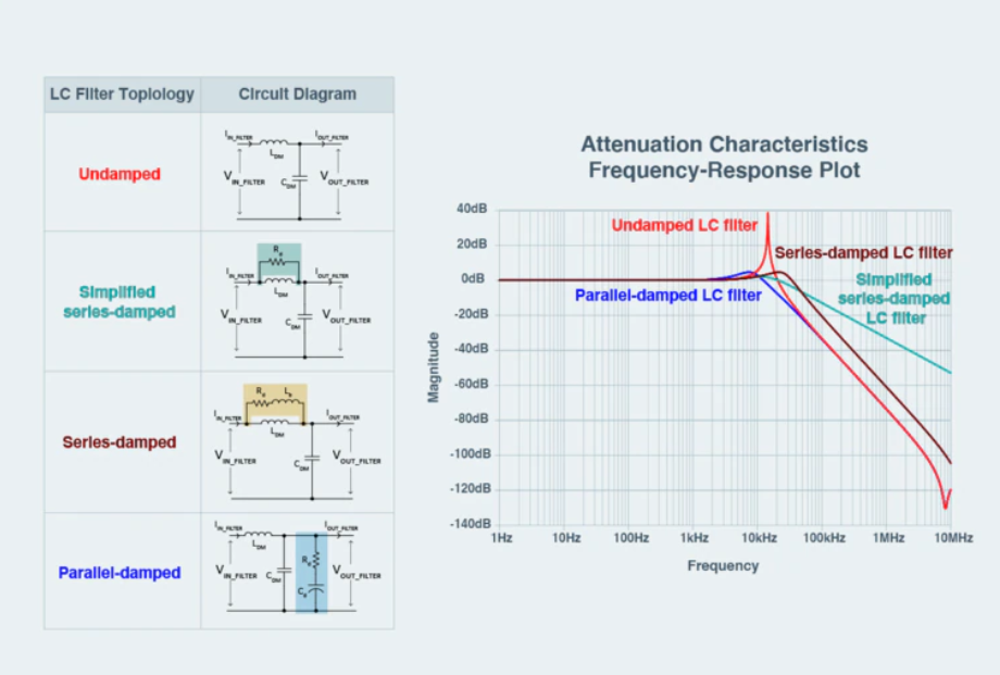
Figure 4: LC filter without damping showing slope of 2nd order attenuation (–40dB/dec) compared with three damping methods.
The second method is to add a damping resistive element and an inductor to the circuit to improve the damping characteristics near the resonance frequency while maintaining the damping characteristics of the second-order filter. However, this method shifts the corner frequency slightly.
A third method is to add a parallel RC damping circuit, which can greatly improve the damping characteristics near the corner frequency of the filter.
Output filter design
Output filter design begins by defining the amount of output voltage ripple that the load can tolerate. Next, consider load current variations (including high di/dt transients). For DC-DC systems feeding highly variable loads, the series inductance of the DC-DC converter's output filter has the greatest impact on the load response performance of the power system.
If the maximum di/dt of the load is defined, we can determine the maximum inductor value for the system. In the equation below, use the di/dt of the load and the maximum voltage drop allowed across the inductor at that time (i.e., the amount of voltage drop below the lowest input voltage at which the load will operate).
Next, after choosing an appropriate inductor, determine the cutoff frequency of the filter from the amount of attenuation required to accommodate the ripple voltage value to the load. From this information, calculate the capacitance of the capacitor using the following formula.
Examination of structure and mounting arrangement
Modern DC-DC switching converters operate at very high frequencies.Therefore, the performance of the filter circuit in the converter system is greatly affected by the parasitic capacitance and regulatory inductance due to component placement and structure.
Basically, the EMI filter is installed near the converter body. In Figure 5, a filtering capacitor is placed close to the input of the DC-DC converter. Due to its proximity to the converter, noise currents circulate locally. When the noise current circulates over a large area, the loop through which the current flows becomes a high frequency antenna, spreading the noise to other parts of the circuit and making the filter useless.
Therefore, both the series filter element and the filter element that shunts the high-frequency current should be placed as close to the DC-DC converter as possible, and the size of the loop through which the high-frequency or large di/dt current passes should be kept as small as possible. To do.
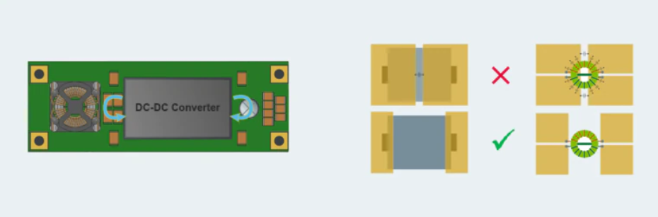
Figure 5: When considering the PCB layout, place the filter element close to the DC-DC converter (left).Separating the copper planes to prevent capacitive coupling prevents noise currents from circumventing high-impedance filter components (right).
PCB layout is also important.Also pay close attention to the noise current path, minimizing the inductance and resistance of the entire noise current path.Take care not to allow high frequency currents to flow through the impedance and create large noise voltages.
Also, the placement of the copper planes on the PCB should be carefully considered to prevent noise from bypassing filtering elements due to parasitic capacitive coupling effects. For example, if the copper planes connecting the terminals of a filter inductor are too close together, high frequency currents will bypass the high impedance inductor through parasitic capacitance. A discretionary placement is to separate the copper planes and minimize parasitic capacitance around series-connected high-impedance elements.
A similar idea applies to common mode chokes. By creating a no-wiring area near the common mode choke winding, parasitic capacitance is prevented and noise does not bypass the filter element.
Filter element performance is highly dependent on environmental and application-specific conditions. For example, the effective capacitance value of a Class 2 ferroelectric ceramic capacitor varies greatly depending on the DC bias voltage.
Here is an example of a 1206 size MLCC. At a DC bias voltage of 50V, the effective capacitance is reduced by 74%. Lowering the effective capacitance raises the corner frequency of the filter, thus reducing the attenuation effect of high frequencies.
Operating temperature can also have a large effect on effective capacitance. Here is an example of the same capacitor. It shows up to a 20% reduction in effective capacitance when used at the upper and lower rated temperatures. When designing filters for DC-DC modules, component performance variability must be assumed and its effects must be considered over the operating range of the system.
Please check the following page of Murata Manufacturing Co., Ltd. for DC bias characteristics and temperature characteristics.
Click here if you want to refer to the DC bias characteristics and temperature characteristics diagrams.
Summary
Attaching an input filter to a power system challenges the stability of the entire power system.The next tutorial will cover stability analysis and decoupling.
Design method of DC-DC system composed of modules
In the previous tutorial, we focused on the advantages of designing a power supply system composed of modules in terms of performance, design flexibility, and development speed, and in the second half, we confirmed the general flow of the design process. The modular approach is good, but requires external circuitry to turn the power distribution network (PDN) into a complete power system. Part 2 of the tutorial addresses the first PDN challenge. Noise filters for the input and output sides of switching DC-DC modules.