
![]()
![]() Narrow down by specifying conditions
Narrow down by specifying conditions
現在1890件がヒットしています。check

Overview
SiC offers many advantages over silicon and is rapidly gaining industry adoption. The high voltage and high speed switching features of SiC enable high efficiency and miniaturization of high voltage and high power applications.
On the other hand, one of the common challenges when upgrading from silicon to SiC is noise and EMI caused by very fast switching speeds. Correct evaluation is important in order to confirm whether correct performance is being achieved.
Macnica has developed and sells a double pulse test board to accurately evaluate the performance of SiC. In this article, we will introduce how to properly measure SiC using this board.
Representative characteristics to be evaluated in experiments
In most cases, the DC characteristics can be read from the data sheet. On the other hand, for AC characteristics, although typical characteristics are listed in the data sheet, they often differ from the application conditions, so it is necessary to actually measure them.
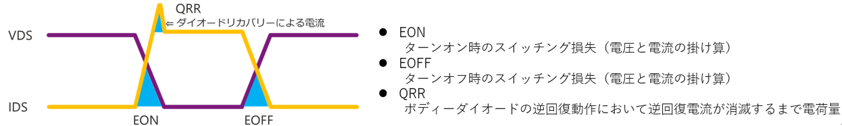
What is especially important is the switching loss EON at turn-on, the switching loss EOFF at turn-off, and the QRR determined from the recovery characteristics of the body diode. All of these parameters require time integration, so the key is how fast and cleanly you can switch. EON and EOFF are directly connected to switching loss, and in the case of PFC circuits where regenerative current flows, the QRR characteristics of the body diode have an effect.
double pulse test
Double pulse tests are commonly used to test the AC characteristics of devices. By connecting an inductive load to a half-bridge circuit and applying pulses multiple times, we can control the current value flowing through the inductive load and observe the switching characteristics at any voltage or current.
Macnica has released a highly versatile double pulse test board so that the TO-247 3-pin or 4-pin devices released as standard by power device manufacturers can be evaluated on a common board.
Macnica double pulse test board overview

■Features
・Supports double pulse test of up to 1700V and 150A
・Through holes compatible with TO-247-4L and TO-247-3L are available.
- Operates with +12V single power supply
・Equipped with adjustable isolated power supply for gate drive
(~25V/ (depending on Zener diode selection)
・Zero bias or negative bias for gate drive can be set with jumper
・Miller clamp Built-in driver I C adopted
・Equipped with connectors and probe contacts for optical insulation probes for VDS and VGS probing.
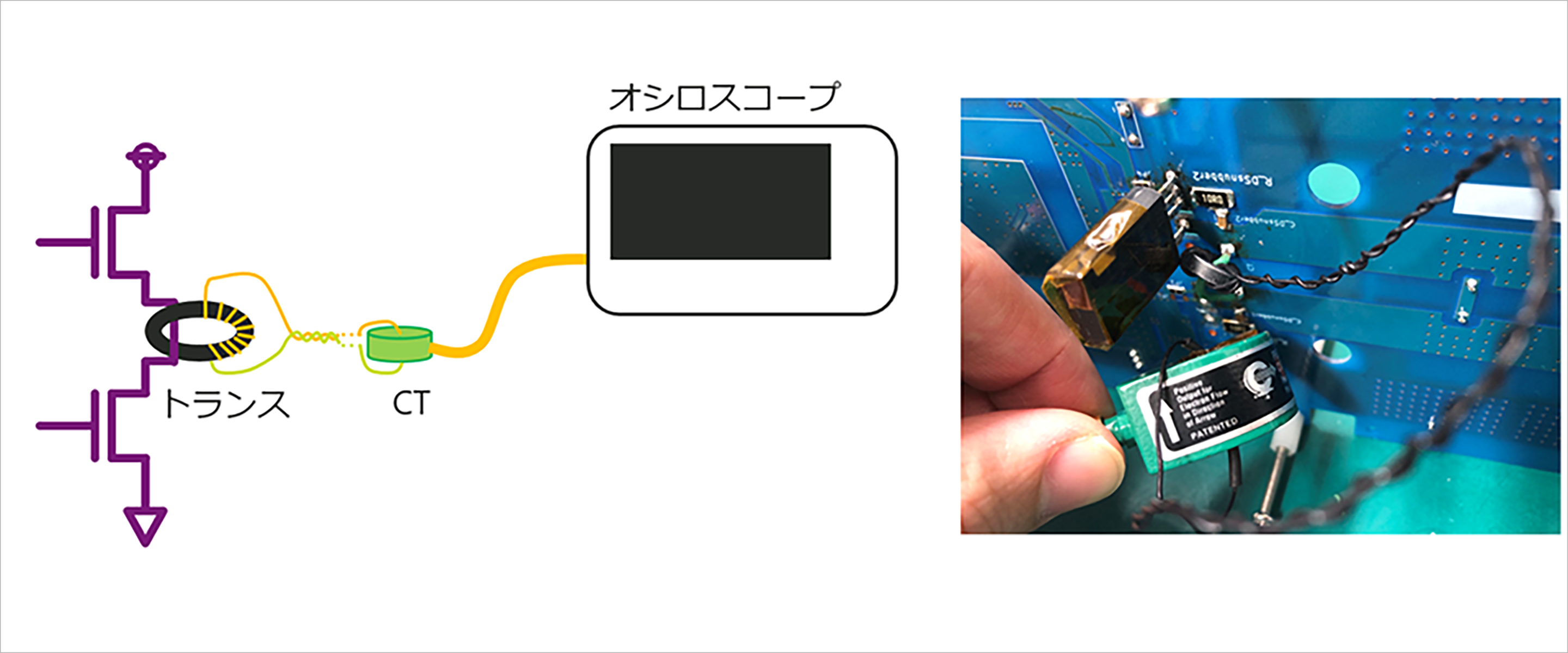
・For current sensor CT, coaxial shunt resistor, and Rogowski coil can be used.
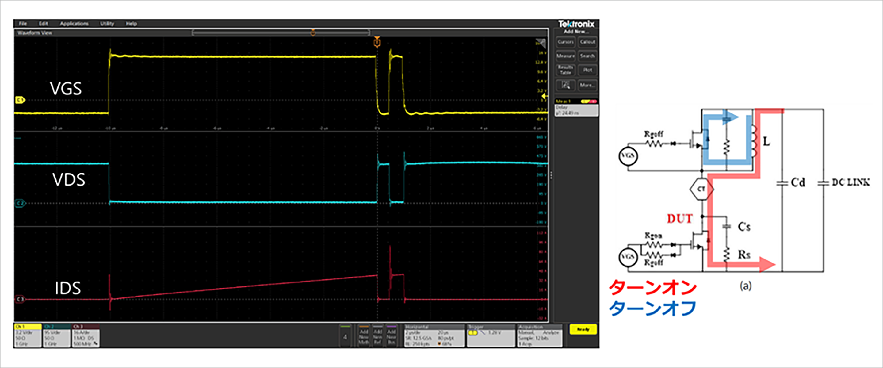
The waveform in Figure 2 is the actual waveform evaluated with Macnica 's double pulse test board. When the device to be measured is first turned on, a current flows from the bus voltage through the inductor and increases proportionally to the pulse width. When the desired current value is reached, turn off and EOFF can be measured from the VDS and IDS waveforms. Then, if you turn it on immediately, you can measure EON and QRR in the same way.
Differences in probes and environments in evaluation
Passive probes, differential probes, optical isolation probes, etc. can be used to measure voltage. Although some passive probes have high frequency bands, they can only measure the low side. Although it is possible to measure the high side using a differential probe, it is not possible to observe the correct waveform due to CMRR.
Also, the leads tend to become long and become antennas. Optical isolation probes are insulated, so they can also measure the high side. Additionally, its extremely high CMRR characteristics allow for the most accurate measurements. The measurement loop can also be made smaller, reducing the effects of noise.
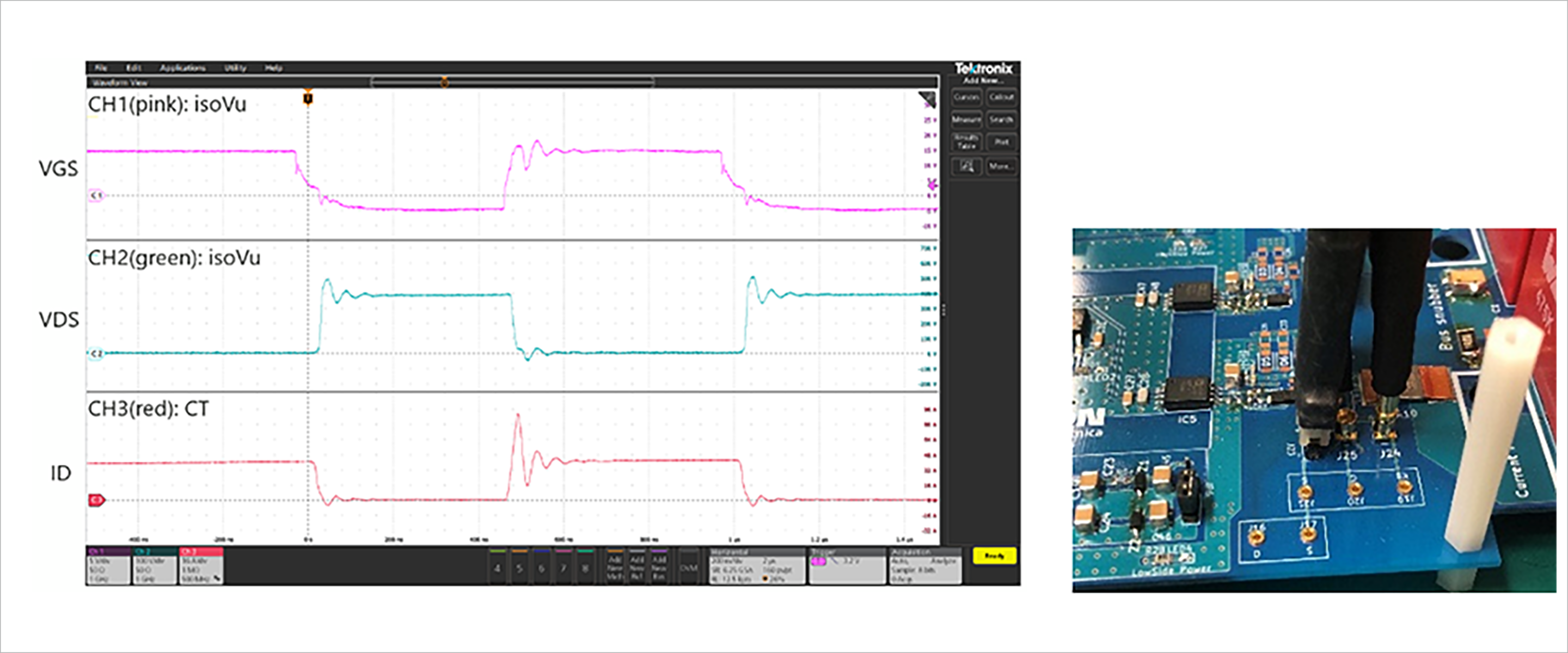
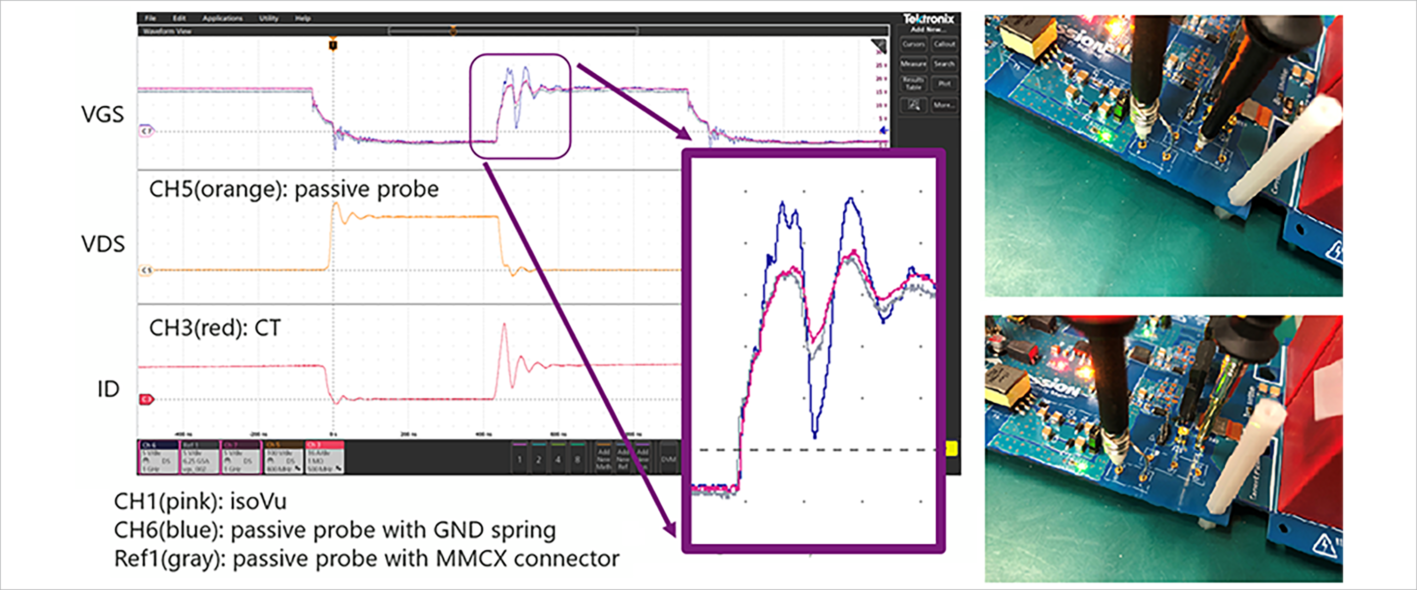
If you only want to observe LowSide, you can observe a sufficiently clear waveform by connecting a passive probe with sufficient bandwidth using the MMCX connector.
Figure 4 shows VGS measured through the GND spring and MMCX connector and compared to the optical isolation probe waveform. While extra ringing is observed with the GND spring, with the MMCX connector a waveform equivalent to that of the optical isolation probe can be observed. It turns out that the probing method is also important.
Please note that MMCX connectors, terminal blocks, film capacitors, etc. are manufactured by Würth Elektronik GmbH & Co. KG.
There are several ways to measure current. To observe waveforms with large currents and high slew rates, it is necessary to measure with the correct equipment. Table 1 shows the typical features of each.
|
Rogowski |
Coaxial |
CT |
|
|
Measuring instrument example |
TRCP0600 |
SDN-414-025 |
PEARSON 2877 |
|
band |
30MHz |
1.2GHz |
200MHz |
|
Ease of use |
Easy to use, but narrow bandwidth. Depending on the mounting location, it may be necessary to modify the board depending on the location. |
Although it has a wide band, it cannot be insulated, so it can only be measured in LowSide mode. It is necessary to secure a place on the board for mounting. |
Can be insulated from the beginning. They tend to be large and difficult to insert into the board, but this can be solved by forming a transformer etc. on the board. |
Table 1: Current measurement methods and their characteristics
Rogowski probes are common and can easily measure current by sandwiching the current path between rings. Although it is easy to use, it does not have much bandwidth and may not be suitable for measuring high-speed devices such as SiC.
Coaxial shunt resistors have a wide bandwidth, but because they cannot be insulated, they can only measure low side. Also, a place for mounting is required on the board.
It is also very difficult to insert a CT into the board, but the problem can be solved by using an external transformer to copy the current and measure the current outside the board.
VGS positive surge and negative surge when switching
When evaluating switching elements, it is also important to evaluate positive and negative VGS surges that can cause false ON and damage. A positive surge occurs when one side of the FET in a half-bridge configuration is switched at high speed, resulting in a very fast DV/DT between the drain and source of the FET that is off, resulting in a voltage drop due to the current flowing through the parasitic capacitance CGD and the gate resistance. Occurs by lifting VGS.
If Vth is exceeded, the device may turn on incorrectly, causing a large current to flow and damaging the device. Negative surges are also generated by charging CGS to the negative side due to steep DV/DT and DI/DT. Negative surges exceeding the VGS rating may damage the device.
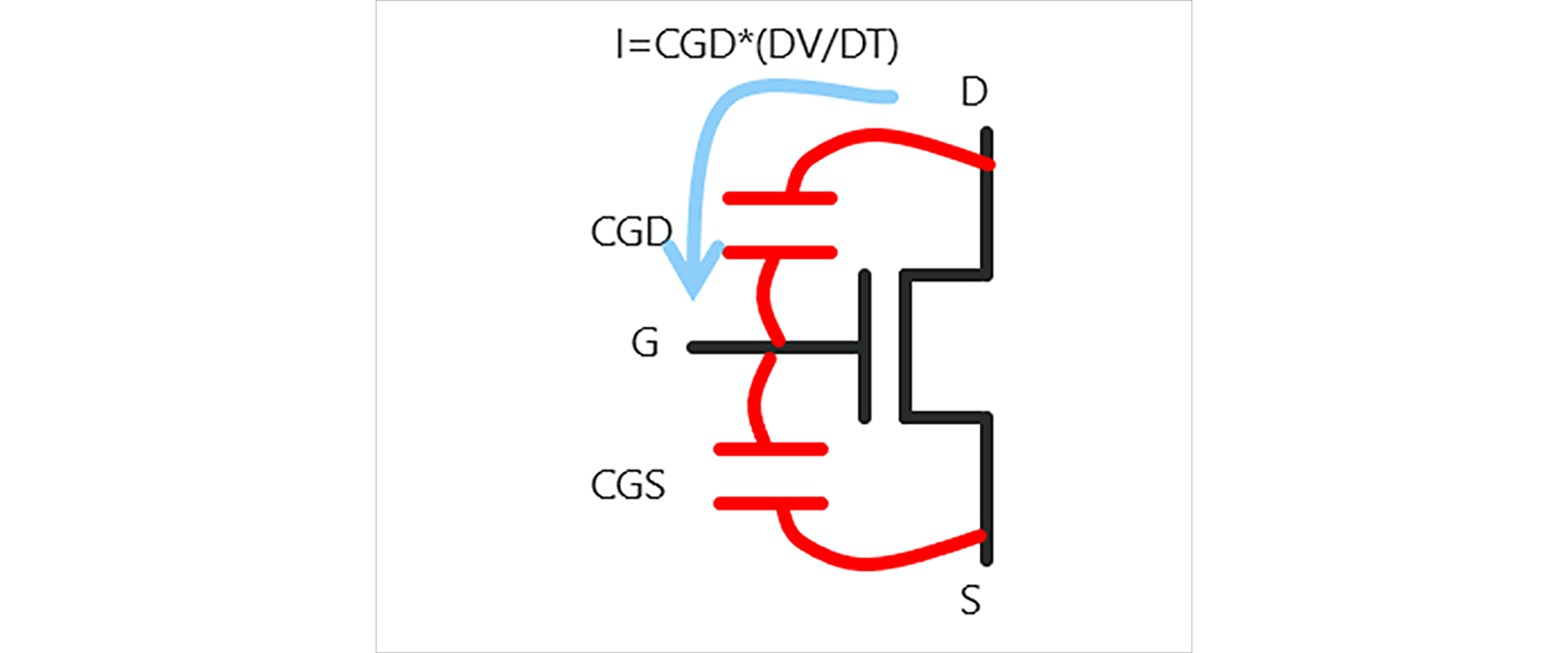
Figure 6: VGS surge causes
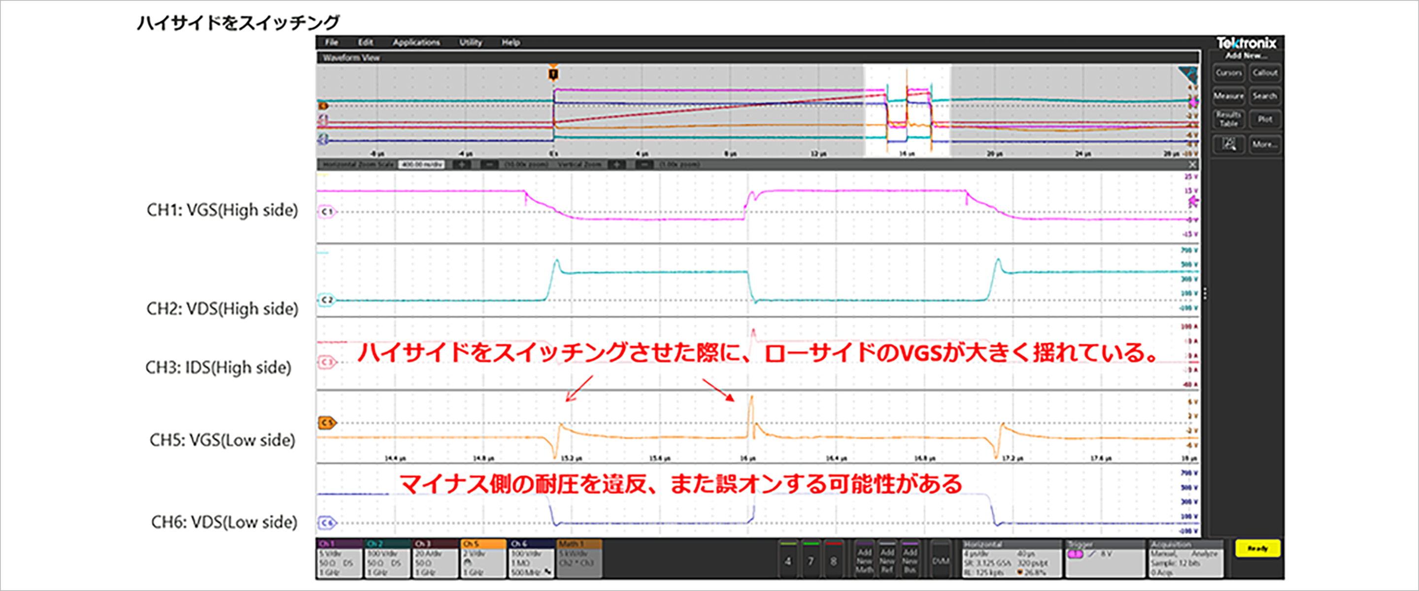
Figure 7 shows the low-side waveform observed during high-side switching using a general SiC MOSFET from Company A. There was no false ON, but the VGS rose close to the gate threshold of the device, and a negative surge occurred that violated the withstand voltage.
There are several techniques to solve these problems. Since the ratio of CGS and CGD affects how VGS fluctuates, adding CGS externally can suppress VGS fluctuations. You can also use the gate driver's Miller clamp to reduce VGS lift. There are also gate drivers that can set the low level of the gate voltage to a negative voltage in order to reduce the possibility of turning on accidentally. You can also add a clamp diode to GND or the negative power supply to suppress negative voltage surges.
Qorvo 's SiC FET has the feature that this problem is less likely to occur. Compared to other companies' products, the CRSS is much smaller, so even if a fast DVDT is applied, the change in VGS can be kept low. In addition, even if a negative surge occurs, Qorvo's gate voltage rating has a wider range than other companies' SiCMOSFETs, so there is a high possibility that the problem will not occur even if you do not take the above measures. .
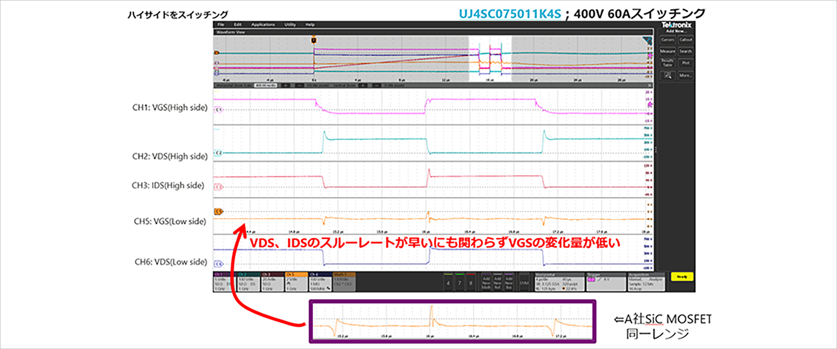
In Figure 8, Qorvo 's 4th generation 750V 11mΩ device is measured using the waveform acquisition conditions of Company A 's SiC MOSFET. Qorvo 's SiC can switch faster than other companies' SiC MOSFETs, but compared to the change in VGS of the SiC MOSFET mentioned earlier, the device's VDS and IDS slew rates are much faster. It can be seen that the amount of change in VGS is low.
Summary
Correct measurement requires a correct measurement environment. Since the conditions for FET specifications vary from company to company, correct measurement under unified conditions is necessary to make correct comparisons. If you can confirm the advantages of Qorvo products through measurement, you may be able to simplify the gate drive circuit and improve system performance.
Macnica 's double pulse test board accurately measures SIC performance and provides an effective environment for selecting the optimal device.
Inquiry
If you have any questions regarding this article, please contact us below.
To manufacturer information top page
If you want to return to Qorvo manufacturer information top page, please click below.
