
![]()
![]() Narrow down by specifying conditions
Narrow down by specifying conditions
現在1888件がヒットしています。check

Overview
Power conversion is a common element in almost all electronic devices and is implemented in various topologies. However, new applications have unique demands that force engineers to develop AC-DC and DC-DC converters with the optimum balance of performance and efficiency. However, this is not always easy.
Choosing the right topology is just the beginning of the challenge and requires careful selection of power components. Also, as new semiconductor technologies enter the market, engineers have the opportunity to discover and evaluate new solutions to traditional problems.
This article provides background on the development of new semiconductor technologies and provides examples of innovative components arranged to provide appropriate functionality for current and future power conversion applications. In three installments, I will explain why high efficiency is necessary, topologies, and figures of merit.
Semiconductor switches and their figures of merit (FoM)
There are various types of semiconductor switches that can be used for LLC converters and similar topologies. Silicon MOSFETs have historically been the standard solution, but their use has some limitations and pitfalls to avoid. The MOSFET output capacitance COSS and stored energy EOSS are highly nonlinear quantities that can be large and require longer than the ideal dead time to discharge. Reliably discharging the energy before switching is important for ZVS, but the action of charging the capacitance dissipates P = fx 0.5 x COSS x V2, and becomes more problematic at higher voltages due to the effect of the V2 term. Masu.
Obviously EOSS should be as low as possible, but that is also a trade-off with on-resistance, other things being equal. Larger dies can have many parallel cells with lower RDS(on) due to lower conduction losses, but naturally higher COSS and thus EOSS. Therefore, FOM RDS*EOSS is important when comparing devices. For similar RDS*EOSS values, another differentiating FOM is RDS-A. A small value means that the device has a small capacitance, and for a given target on-resistance, the yield from the wafer is high, resulting in a low unit price.
Body diode and diode effect characteristics are important when comparing devices. In resonant converters, the intrinsic diode of the MOSFET conducts naturally during soft switching, but has relatively poor performance such as high forward voltage drop, slow charge recovery QRR, and incomplete switching cycles at high frequencies with short dead times. and loss may occur. Wide bandgap devices, such as gallium nitride (GaN) HEMT cells, do not have a diode and conduct in the "third quadrant" from source to drain through the main channel rather than the parasitic diode found in MOSFETs. Although there is no charge recovery in the 3rd quadrant conduction of the HEMT cell, the forward voltage drop is also very large, resulting in a negative off-drive voltage in addition to the turn-on threshold voltage of the gate.
WBG Silicon Carbide (SiC) technology MOSFETs have fast parasitic diodes like Schottky diodes, but they also have a high forward voltage of about 3V. Although conduction time in the third quadrant is short, diodes and diode effects can lead to significant losses when the highest efficiency is desired. RDS*QRR is a useful FOM as a measure of the combined channel conduction and diode losses. Also, SiC MOSFETs and GaN HEMT cells have very sensitive gate drive requirements for optimum efficiency.
A device that has all the characteristics is the SiC FET (Fig. 1). Combining low-voltage Si-MOSFETs and SiC JFETs in a cascode configuration, RDSA, RDS*EOSS, and RDS*QRR have similarly lower FOMs than Si superjunction MOSFETs, SiC MOSFETs, and GaN HEMT cells. It is
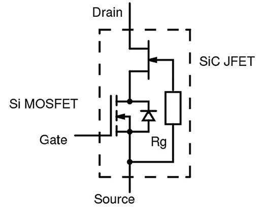
SiC FETs feature the advantages of SiC, such as ultra-fast switching, high thermal conductivity, and high temperature operation, as well as easy gate drive like low-voltage Si-MOSFETs. The device's capacitance and stored charge are all low, it has a body diode effect, it is fast, and it has a low forward voltage drop of about 1.5V at 25°C. Also, unlike GaN devices, they avalanche and are current limited under short-circuit conditions.
new solution
SiC FETs are now being recognized for their superiority in high-efficiency DC-DC converter applications using LLC and PSFB topologies. Taking advantage of this low loss, converter size, especially height, has been reduced, enabling tight module packaging and increased system power density. For such applications, SiC FET power switches are the only option in surface mount packages, traditionally D2PAK-3L and D2PAK-7L. These devices support high current ratings, most notably the -7L package rated to 1700V and employs a Kelvin source connection to counteract the effects of lead inductance. But the height is still close to 0.19in (5mm).
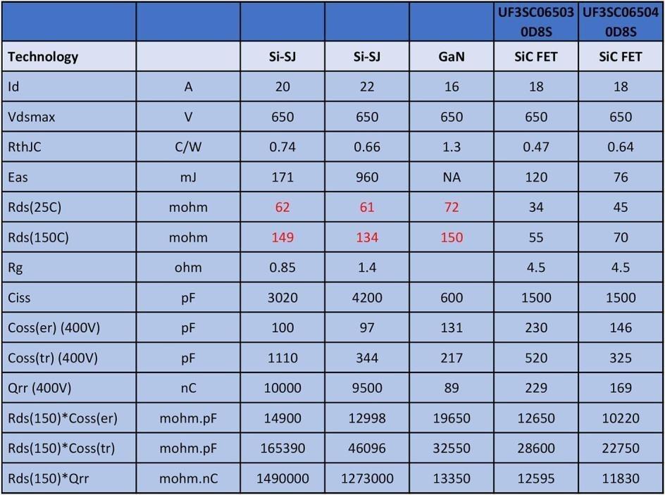
Qorvo's new solution is a SiC FET family housed in a DFN 8x8-4L package with a maximum height of 0.043 inches (1.1mm) and an 8mm square size. The device has a voltage rating of 650V and an on-resistance of 34 or 45mΩ at 25°C. Also, like other SiC FET devices, it has easy 0-10V gate drive, ultra-fast switching, low QRR, and robust body-diode effect when zero-voltage switching is lost. The figures of merit for RDS*EOSS and RDS*QRR are the lowest in their class compared to 650V silicon superjunction MOSFETs and GaN HEMT cells (Table 1). Sintered silver die attach provides the lowest case thermal resistance, combined with SiC's inherent high temperature performance, ESD protection, and excellent avalanche and short-circuit behavior make for a robust product .
Conclusion
Efficiency drives all modern power converter designs because of the energy and cost savings and miniaturization that can be achieved with less power loss. Modern circuit topologies with resonant switching routinely achieve efficiencies in the high 90s, with the remaining losses concentrated in residual conduction and switching effects. Wide bandgap semiconductor switches, such as SiC FETs, have emerged to further reduce loss, and have achieved on-resistance in milliohm units and switching characteristics that are close to ideal. Combined with the ease of circuit implementation, the availability of parts in ultra-low profile packages like Qorvo's DFN 8x8 makes them high-performance, robust solutions for low-loss power switching.
Inquiry
If you have any questions regarding this article, please contact us below.
Qorvo manufacturer information top page
If you want to return to Qorvo manufacturer information top page, please click below.
