
![]()
![]() Narrow down by specifying conditions
Narrow down by specifying conditions
現在1888件がヒットしています。check

Overview
Power conversion is a common element in almost all electronic devices and is implemented in various topologies. However, new applications have unique demands that force engineers to develop AC-DC and DC-DC converters with the optimum balance of performance and efficiency. However, this is not always easy.
Choosing the right topology is just the beginning of the challenge and requires careful selection of power components. Also, as new semiconductor technologies enter the market, engineers have the opportunity to discover and evaluate new solutions to traditional problems.
This article provides background on the development of new semiconductor technologies and provides examples of innovative components arranged to provide appropriate functionality for current and future power conversion applications. In three installments, I'll discuss why you need high efficiency, topologies, and figures of merit.
transformation topology
There are many topologies for DC-DC conversion to produce the final load voltage, depending on the power level and whether isolation is required for safety or functional reasons. Apart from non-isolated and inefficient linear regulators, switch-mode regulators are popular for achieving high efficiency, and their topologies consist of two basic configurations.
Topologies consist of two basic configurations: "buck" or "boost" (Figure 1). A buck converter outputs energy directly in pulses, with an energy storage inductor supplying current to the output during the off-time of the main switch. A boost converter stores all the energy needed for the output in an inductor when the main switch is on, passes that energy to the output when the switch is off, and in both cases has a capacitor that smoothes the output to DC. In an isolated converter, the principle is the same as in the equivalent transformer-coupled topologies "forward" and "flyback" converters.
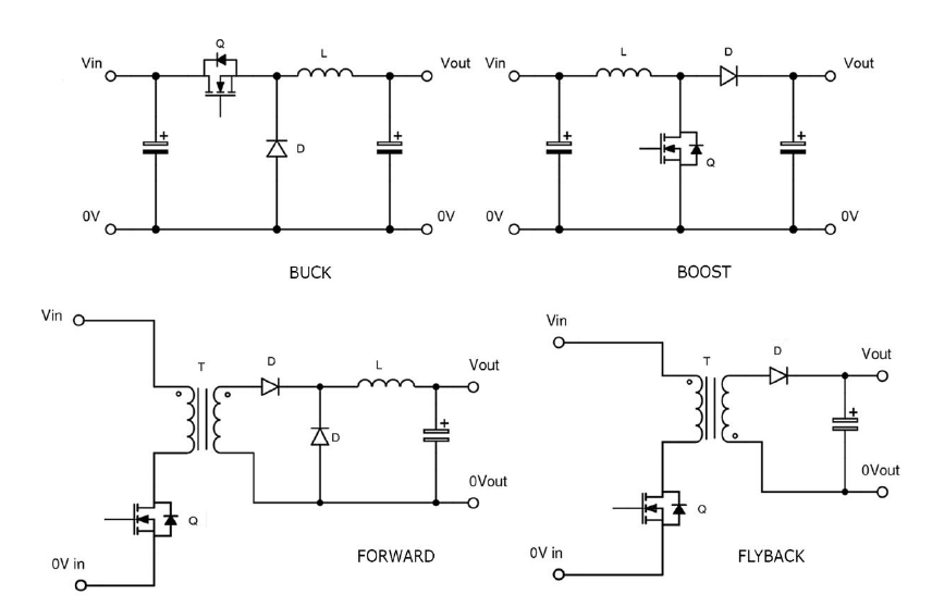
Buck converters are by far the most popular at power levels of tens of watts and above for both isolated and non-isolated applications. This is because the size of the magnetic components in a step-up converter tends to be proportional to the power, whereas in a step-down converter this trend is weaker, and practicality such as wire size and insulation distance largely affects the overall size of the magnetic components. to influence. A non-isolated buck converter supports high output with low loss by adding functions such as synchronous rectification by replacing the diode in Fig. 1 with a MOSFET. In polyphase versions, two or more power stages are driven out of phase to distribute the stress on the semiconductors, and the latest generation wide bandgap (WBG) semiconductors reduce conduction and switching losses. Isolated converters offer a wider choice of buck topologies, from single-switch types to half-bridges to full-bridges, coupled with synchronous rectification to allow the use of multi-phase arrays at higher power levels.
These topologies can dissipate power during switch transitions where voltage and current are high at the same time. To address this issue and increase efficiency, "resonant" or "soft-switched" designs have been developed, which can delay the current rise until the voltage drops to zero when the switch is turned on ( Zero Voltage Switching: ZVS). Similarly, zero-current switching (ZCS) is possible when the switch is off. Achieving ZVS and ZCS at the correct timing is difficult under all conditions, including changes in device characteristics due to input, load, time, and temperature. At high power, the resonant PSFB (Phase Shifted Full Bridge) is popular, it is easy to drive a switch with a 50% duty cycle, and the regulation is achieved by changing the phase of the gate drive pair in the bridge arrangement. .
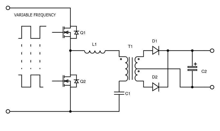
At moderate power, the LLC series of resonant converters (Figure 2) has become the standard for high efficiency, and here too it is easy to drive the gates with a 50% duty cycle into half or full bridges. Regulation is achieved by varying the switching frequency within a relatively narrow range.
The adoption of complex resonant designs such as PSFB and LLC types is also facilitated by the introduction of digital control techniques that give flexibility to adapt circuit dynamics to changing conditions in order to achieve high efficiency throughout the operating range. .
LLC converter
A closer look at this LLC converter shows how this topology enables the low power consumption of solid-state switches. In the schematic circuit of Figure 2, the two switch gates are driven out of phase with a 50% duty cycle to drive a simple square waveform across the resonant circuit or "tank" formed by L1, C1 and the primary inductance of transformer T1. supply. Simply put, the tank and the reflected load on the transformer form a voltage divider, and at resonance the tank becomes a resistance, a minimum, so there is no damping. At high or low frequencies away from resonance, the tank impedance becomes capacitive or inductive, with variable damping, but peaks at the main resonant frequency, which is load dependent.
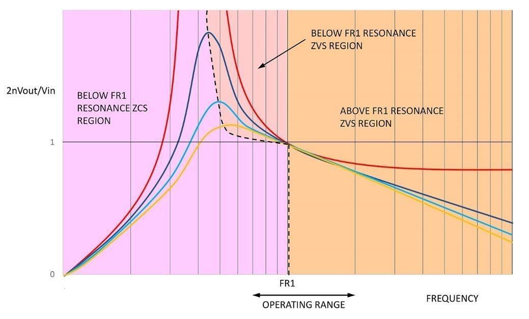
This allows the output voltage to be controlled by varying the drive frequency. It also has the effect that the tank circuit filters the square wave drive to produce essentially sinusoidal currents in the transformer primary and secondary. Therefore, no inductor is required for the output filter. In practice, there are two resonances formed by L1/C1 and L1, the magnetizing inductance of the transformer, and C1, which complicates the change in gain with the power supply circuit (Figure 3). A practical circuit operates around the resonance Fr1 of L1/C1 in Figure 3.
Both primary switches are capable of zero volt switching. Briefly again, with an inductive load, the current lags the voltage, so if you operate the LLC converter above the main resonance where the tank appears inductive, the current will rise only after the voltage, with minimal overlap and dissipation. will be limited. After Q1 turns off, the energy stored in the magnetizing inductance causes a reverse current to flow through switch Q2 during the dead time before Q1 turns on, discharging the capacitance at the common junction of the switches. This is a requirement for ZVS, and the ZVS mechanism is the same whether Q1 is on or Q2 is off. Zero current switching of the output diode occurs naturally.
However, when forced to operate at low frequencies in capacitive regions where current exceeds voltage, ZVS can be lost during overload or short circuit, resulting in lossy "hard switching". Losses also occur at light loads when the energy stored in the inductance is not sufficient to discharge the switching node capacitance. Therefore, semiconductor switches with minimal output capacitance and corresponding EOSS are preferred for the lowest loss switching under all normal conditions, and low recovery when ZVS is lost under abnormal conditions. A fast body diode with charge QRR is required.
Inquiry
If you have any questions regarding this article, please contact us below.
Qorvo manufacturer information top page
If you want to return to Qorvo manufacturer information top page, please click below.
