- Semiconductor BusinessHOME
- Products and Services of Macnica,Inc.
-
technical information

-
Events and Seminars
- Handling Manufacturer
- Support
- Inquiry
- Click here to purchase products
- Semiconductor business e-mail magazine registration
![]()
![]() Narrow down by specifying conditions
Narrow down by specifying conditions
現在2182件がヒットしています。check

Why SiC Cascode JFETs are an Easy Replacement
ON Semiconductor's SiC cascode JFET product lineup is built on a core technology that combines a high-voltage normally-on SiC JFET with a low-voltage normally-off Si MOSFET in a cascode configuration.
ON Semiconductor's SiC cascode JFET is cascode connected, making it easy to drive. Figure 1 is a simplified diagram of the cross-sectional structure of a typical SiC MOSFET and ON Semiconductor's SiC cascode JFET. Generally, a SiC MOSFET requires a negative voltage such as -5V to turn it completely off, and a high voltage such as +15V to turn it completely on.
Additionally, there are some products that can only tolerate an absolute maximum VGS rating of -7 V. This is due to the channel structure of typical SiC MOSFETs, which does not have any margin for the absolute maximum VGS rating.

Figure 1. Schematic cross-section of a typical SiC MOSFET and ON Semiconductor's SiC cascode JFET
Figure 2 shows the recommended VGS operating voltage and absolute maximum voltage rating for each device.
As can be seen from this graph, typical SiC MOSFETs are used under tight operating conditions, and exceeding the absolute maximum rated voltage will have an impact on the device's lifespan. Looking at ON Semiconductor's SiC cascode JFETs, the recommended VGS operating voltage is 0 to 12V, and the absolute maximum rated voltage is ±20V, which is on the same level as typical Si MOSFETs. ON Semiconductor's SiC cascode JFETs are significantly more robust than SiC MOSFETs, allowing for a wider range of gate drive circuit options.

Figure 2. VGS recommended operating voltage and VGS absolute maximum rated voltage for each power device
ON Semiconductor's SiC cascode JFETs can be easily replaced by conventional power devices because the gate drive circuits can be used as is.
The most important factor when considering a drop-in replacement for an existing device is the gate drive voltage. The VGS absolute maximum rated voltage for Si MOSFETs and Si IGBTs is generally ±20V. Some conventional Si MOSFETs have a negative limit of -5 to -10V. In addition, the gate threshold voltage is approximately 5V, and since they are normally OFF, no negative drive voltage is required. To turn them ON, typically +12V to +15V is required.
On the other hand, typical SiC MOSFETs have a low gate threshold voltage of approximately 2.2 V. To avoid false turn-on, they require a negative gate voltage when turned off, and a voltage of +15 V to +20 V to fully turn on.
ON Semiconductor's SiC cascode JFETs have a gate threshold voltage of 5V, the same as Si devices, and are normally OFF. No negative voltage is required for gate drive. They can also be driven at 12V, allowing them to replace Si MOSFETs and Si IGBTs. Of course, they have sufficient voltage resistance in the negative voltage direction, so there is no problem using a drive circuit that swings from -5V to +20V to drive a typical SiC MOSFET. ON Semiconductor's SiC cascode JFETs can easily replace SiC MOSFETs, Si IGBTs, or Si MOSFETs.

Figure 3. Comparison of ON Semiconductor's SiC cascode JFET and SiC MOSFET
ESD Tolerance of SiC Cascode JFET
In a cascode configuration of a SiC JFET and a Si MOSFET, the Si MOSFET is connected to the gate and source terminals of the package, which limits its ESD performance. The JFET is a PN junction and can handle much more ESD than a MOSFET. ON Semiconductor's MOSFETs use an integrated diode for ESD protection, and the size and capacitance of the Si MOSFET are the determining factors for ESD performance.

Figure 4. Basic cascode configuration with Si MOSFET drain connected to SiC JFET source (left).
Cascode configuration with back-to-back diodes from Si MOSFET gate to source pad (right)
Across ON Semiconductor's SiC cascode JFET product lineup, we use a family of MOSFETs scaled to match the size and RDSon of the JFET. The smallest JFETs require the smallest MOSFETs, and these limit the ESD rating of the part. This also means that ESD testing the MOSFET alone determines the ESD rating of all products using that MOSFET.
In the charged device model, all MOSFET samples were tested to ±2000V and passed. This places the parts in CDM Class C3 (>1000V). In the human body model, all MOSFET samples were tested to a maximum of ±8000V for each of the three terminal combinations. All MOSFETs passed up to 8000V for the drain-source terminal pair. Gate-source and gate-drain tests vary depending on the device size. The smallest MOSFETs passed 3900V gate-source and 3700V gate-drain.
SiC JFET ESD rating
ON Semiconductor's SiC JFETs are scaled in size, with the smallest devices being the most sensitive to ESD. Unlike MOSFETs, JFETs are constructed with PN junctions and are therefore inherently insensitive to ESD. Utilizing the smallest JFET in the lineup, charged device model testing was performed up to ±1000V, and human body model testing of all terminal pairs was performed to ±8000V. All JFETs are C3 and H3A class, respectively.
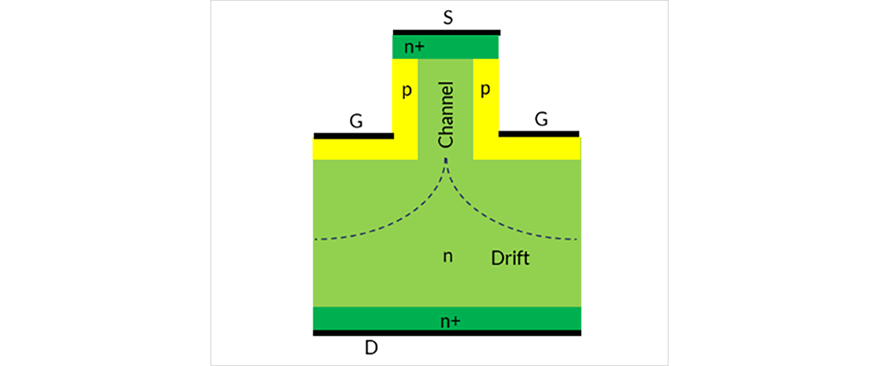
Figure 5: Unit cell in JFET structure with (a) no gate oxide and (b) two PN junctions (gate-drain and gate-source) highlighted.
Inquiry
If you have any questions regarding this article, please contact us below.
On Semiconductor Manufacturer Information Top Page
If you would like to return to the ON Semiconductor manufacturer information top page, please click below.