- 半導体事業HOME
- マクニカの製品・サービス
-
技術情報

-
イベント・セミナー
- 取扱メーカー
- サポート
- お問い合わせ
- 製品購入はこちら
- 半導体事業のメルマガ登録
![]()
![]() 条件を指定して絞り込む
条件を指定して絞り込む
現在2168件がヒットしています。check
はじめに
シリコンの一般的な光デバイスはフォトダイオード(PD)が知られていますが、感度が高くなるとアバランシェフォトダイオード(APD)、シングルフォトンアバランシェダイオード(SPAD)が出てきます。SPADはマルチアレイ化が進み、SiPMと呼ばれ、近年、医療機器やLiDARセンサーとして採用さるようになっています。
この記事ではSPADがどのようなデバイスかを説明します。
PD, APD, SPADの特徴
PD, APD, SPADの基本構造はPNジャンクションで構成されており、どの逆バイアス条件で動作させるかでデバイス名称が変わります。
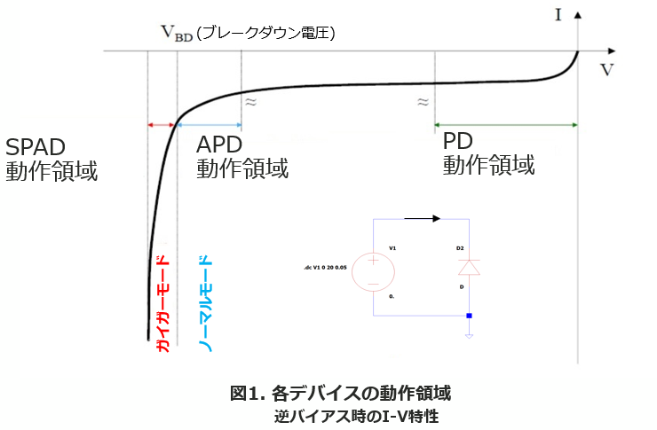
図1は各デバイスの逆バイアス時の動作領域を示しています。軸はX,Yともにリニアです。図からわかる通り、PD,APDは線形領域で動作するデバイスです。SPADは非線形領域で動作し、その領域をガイガーモードと呼んでいます。このガイガーモード動作は高速かつ超高増率の特徴を持ちます。
光電流発生モデル
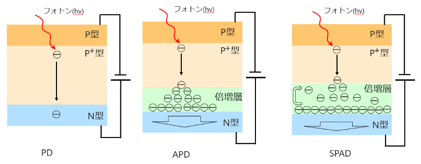
図2で簡単に光発生電流の説明をします。
PDでは1フォトンに対し1電子しか発生しません。APDはVBD近辺で動作しますので、1フォトンでアバランシェ電流が発生します。ただし、100個程度の電子の発生になります。SPADはVBD以上のバイアスで動作させますので、運動エネルギーの大きい電子がさらにアバランシェ電流を発生させます。複数のアバランシェ電流が発生し、100万個の電子に到達します。
APDの動作をノーマルモード、SPADの動作をガイガーモードとするとバイアスと増幅率は、次の関係式になります。
ノーマルモード: Vr<VBR 増幅率<100
*入力光子数に増幅率は比例。
ガイガーモード: Vr>VBR 増幅率≒100万
*必ず1光子は100万倍に増幅され発生した電子が吐き出されるまで次の入力光子の影響を受けることがないのがガイガーモードの特徴になります。
ToFセンサーとしてのSPAD(SiPM)
単純にPDの高感度デバイスとしてなら注目を浴びることもないのですが、抵抗を内蔵するだけでToFセンサーとして使うことができるのも特徴の一つです。ここでは、簡単にToFセンサー動作の説明をします。
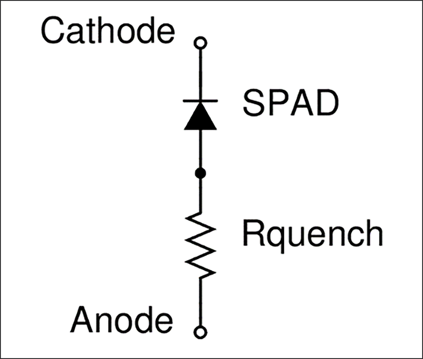
図3は単体SPADの等価回路図です。等価回路にある内部抵抗はクェンチ抵抗と呼び、これが放電抵抗の働きをします。図4は、ガイガーモードで、クェンチ抵抗を付加したときの放電サイクルになります。フォトンが入射するごとにこのサイクルを繰り返します。
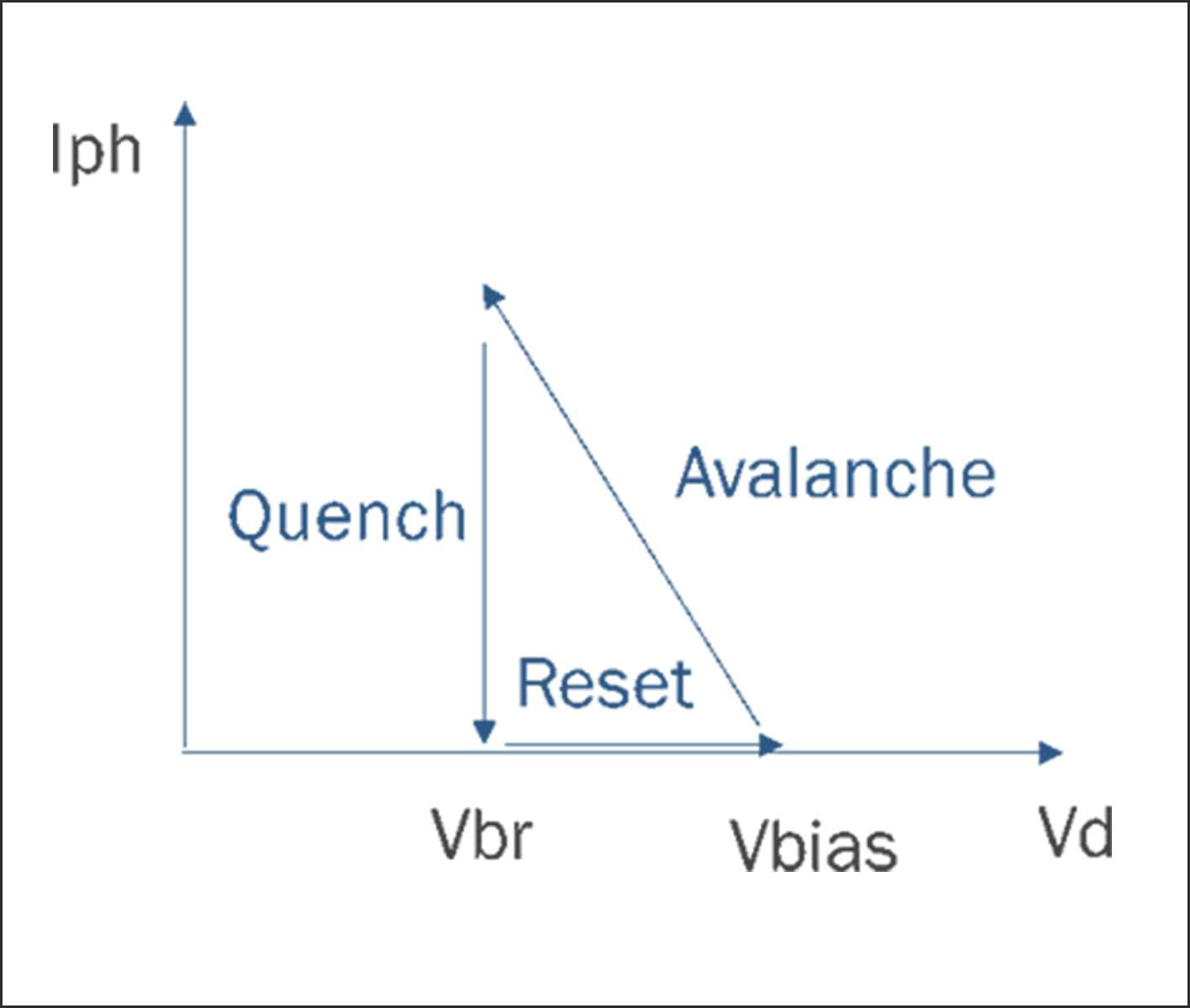
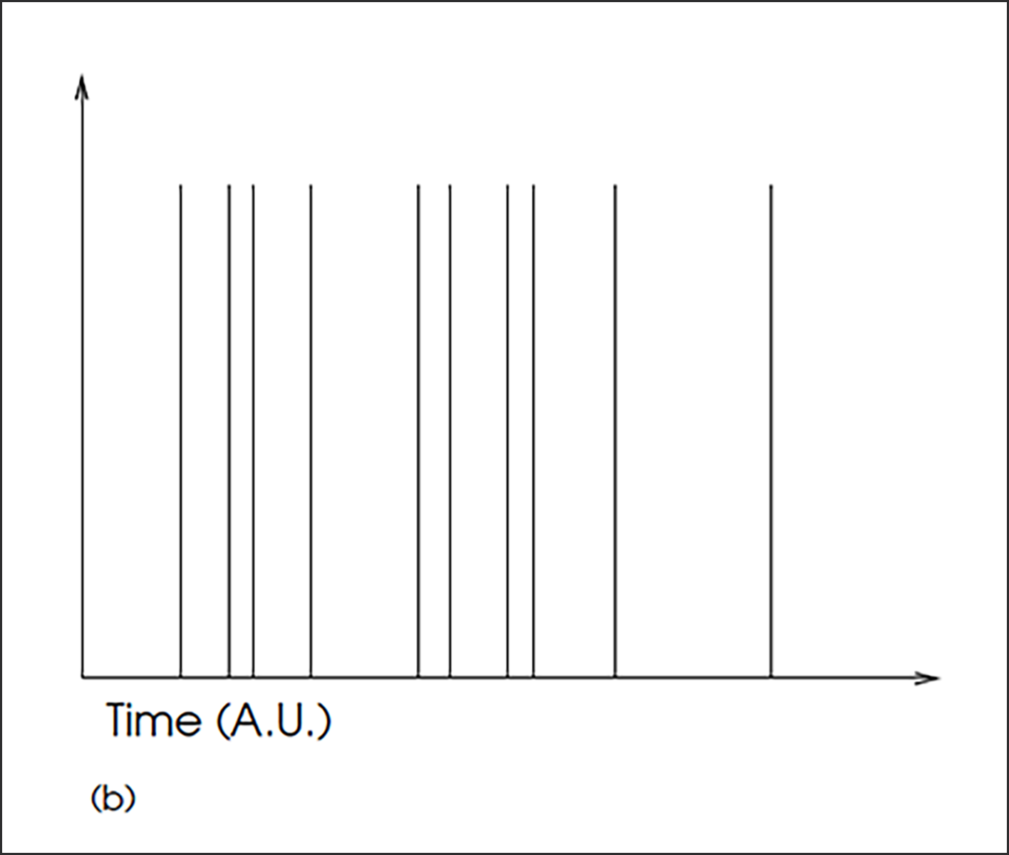
さて、フォトンは時間をかけて飛び込んでくるので、図4での放電電流をI-V変換アンプで電圧出力すると図5のようになります。縦軸が電圧です。横軸は光源から射出したフォトンが反射で入力されるまでの時間を表しています。まだこのままでは対象物の距離が分かりません。
実際の測距は射出パルスの立上り時間t1、反射波パルスの立上り時間t2とすれば、”対象物までの距離=(t2-t1)*光速/2“となります。例えば、(t2-t1)が2nsとすれば対象物までの距離は30cmになります。
今までは単体センサー説明でしたが、センサーをアレイ化した場合、SiPMとした場合は何が測れるのでしょうか?
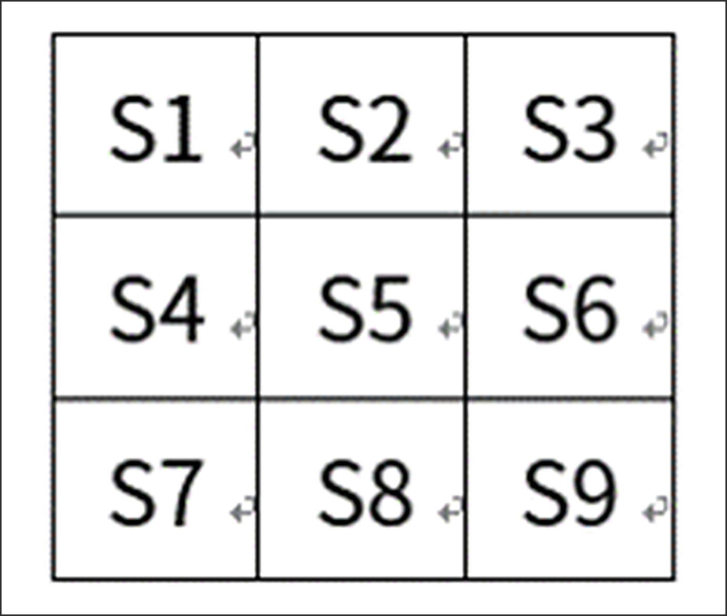
例として図6のように、9個のセンサーがアレイ化されたとします。そして各セルは出力端子を持っています。また光源は単一パルス光源とします。すべてのセルの(t2-t1)が同じであれば対象物は平面だと判断できます。各セルの(t2-t1)が異なる場合は、夫々の距離をマッピングすると、対象物の3D(曲面もしくは凸凹)情報が得られます。
気づかれた方もいると思いますが、アレイ化センサーはdToFセンサー動作することがわかります。このセンサーのアレイ化(ピクセル数)を増やすことで、また光源パルスの射出(スキャン)回数を増やすことで、より繊細な3D画像が構成でき、対象物が人なのか、動物なのかあるいは何かの建築物なのか判定できるようになります。
オンセミ社SiPM一覧はこちら、オンセミ社のWebサイトの製品ページをご確認ください。
オンセミ社LiDAR評価キットご購入検討の方はこちら、オンセミ社のWebサイトをご確認ください。
お問い合わせ
今回紹介した内容及び製品にご興味がある方は、ぜひお問い合わせください。
オンセミ メーカー情報Topへ
オンセミ メーカー情報Topに戻りたい方は以下をクリックしてください。