- 半導体事業HOME
- マクニカの製品・サービス
-
技術情報

-
イベント・セミナー
- 取扱メーカー
- サポート
- お問い合わせ
- 製品購入はこちら
- 半導体事業のメルマガ登録
![]()
![]() 条件を指定して絞り込む
条件を指定して絞り込む
現在2179件がヒットしています。check

パワーコンバーターの設計者に、半導体スイッチに何を求めるかを尋ねると、次のような答えが返ってくるかもしれません。「低オン抵抗、高オフ抵抗、そして2つの状態間の可能な限り早い遷移」。もちろん、単純に考えれば、これは低消費電力につながるということです。オンセミのSiCカスコード JFETは、この理想に近いもので、オン抵抗は750Vクラスで6mΩ以下、エッジレートはナノ秒領域で、数kWクラスのコンバーターやインバーターで99.5%以上の効率が期待できます。
設計者は、容易なゲート駆動、高電圧定格、効率的な第3象限動作、高いアバランシェエネルギーと短絡定格、低熱抵抗、低システムコストなど、いくつかの「ついで」を入れることを考えるでしょう。幸いなことに、SiCカスコード JFETはこれらの要素もカバーしており、クラス最高レベルの性能指数を備えています。
しかし、SiCカスコード JFETをブレッドボード上で最大のスルーレートで動作させると、すぐに煙が出てしまうのです。「電源電圧は最大値を大きく下回っていたし、負荷も軽かったのに。」さて、どれだけの配線と接続インダクタンスがあったのでしょうか?たった100nHのインダクタンスでも3000A/µsという驚異的な電流エッジレートでは、おなじみの方程式V = -L*di/dtから300Vの電圧スパイクを発生させ、スイッチにストレスを与えます。SiCカスコード JFETが壊れるまでのわずかな期間ですが、マイクロ秒の高周波リンギングを誘発したのです。
現在では、接続インダクタンスをゼロにするか、スイッチの定格電圧を大幅にオーバースペックにしてEMIフィルターを多用しない限り、エッジレートを制御してリンギングを減衰させる必要があることがわかっています。電圧スパイクを抑制する従来の方法は、ゲート抵抗RG(OFF)を直列に追加することでしたが、これには問題があり、波形に遅延が生じて、ワイドバンドギャップスイッチの最大の利点の1つであるデューティーサイクルや高周波動作が制限されます。また、ゲート抵抗はスイッチの損失を大幅に増加させるだけで、リンギング減衰効果はほとんどありません。
より良い解決策は、シンプルなRCスナバです。一般的にIGBTで必要とされる、大きくて熱い抵抗とコンデンサーのネットワークは敬遠されるかもしれませんが、SiCカスコード JFETの場合は違います。スナバは主に、接続インダクタンスとデバイスのキャパシタンスとの間の共振を減衰させるために使用されますが、SiCカスコード JFETのキャパシタンスは非常に小さいのです。つまり、200pF程度の容量(Coss(er)の2倍または3倍)と数Ωの直列抵抗があれば、一般的には十分なダンピング効果が得られるということになります。一部の電力はスナバ抵抗で消費されますが、このネットワークはハードスイッチとソフトスイッチの両方のアプリケーションで、スイッチオフ電圧と電流のオーバーラップを減らす働きをするため、実際にはこの移行時の損失は少なくなります。
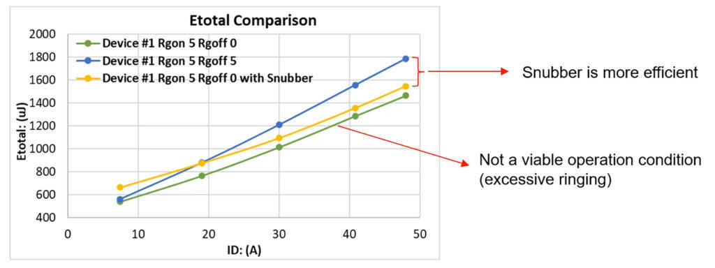
スナバはターンオン時に若干の損失が発生しますので、全体像を把握するためには、トータルロスE(ON)+E(OFF)を考慮する必要があります。図は、40mΩの場合のE(TOTAL)を示しています。青い線はスナバがなく、RG(ON)、RG(OFF)ともに5Ωの場合です。黄色い線は、RG(ON)が5Ω、RG(OFF)が0Ωで、200pF/10Ωのスナバを使用した場合です。40Aでスナバを使用すると、40kHzで動作しているときに約10.9Wの損失削減という明らかな純利益が得られます。軽負荷時には状況が逆転しますが、このレベルでは損失は少ないです。
一般的なアプリケーションでスナバ抵抗に吸収されるエネルギーを評価すると、1サイクルあたり約120μJとなり、40kHzでは約5Wに相当します。しかし、評価の結果、このエネルギーのほとんどは、スナバ抵抗ではなく、ターンオン時にSiCカスコード JFETのチャネルが線形領域を通過する際に消費されることがわかりました。その結果、スナバには通常1Wの抵抗器で十分であり、この電力レベルでは表面実装タイプの抵抗器が容易に使用できます。また、コンデンサーも小さくできます。
設計者は、他の利点を損なうことなく、オーバーシュートやリンギングを減らすために、スナバ回路を足すことで簡単かつ安価に調整できます。
お問い合わせ
本記事に関してご質問などありましたら、以下より問い合わせください。
オンセミ メーカー情報Topページへ
オンセミ メーカー情報Topページへ戻りたい方は、以下をクリックください。