- Semiconductor BusinessHOME
- Products and Services of Macnica,Inc.
-
technical information

-
Events and Seminars
- Handling Manufacturer
- Support
- Inquiry
- Click here to purchase products
- Semiconductor business e-mail magazine registration
![]()
![]() Narrow down by specifying conditions
Narrow down by specifying conditions
現在2189件がヒットしています。check

Introduction
Applications using SiC semiconductors began in the 2000s with the adoption of SiC JBS diodes for PFC (Power Factor Correction) applications. Later, SiC diodes and FETs were used in the PV (photovoltaic) industry. Going forward, the recent surge in applications related to EV on-board chargers and DC-DC converters is expected to drive the growth of SiC semiconductors. The early adoption of 650V devices for EV inverters and server power supplies and 5G telecom rectifiers promises a rapid future growth for SiC semiconductors. This article discusses the advantages of rapidly growing SiC semiconductors over current Si technology.
Advantages of SiC semiconductors
The advantages of using SiC FETs over IGBTs are well documented. The wider bandgap of 4H-SiC allows the formation of a voltage blocking layer with resistance about 100 times lower than unipolar silicon devices. SiC semiconductors also have three times the thermal conductivity of silicon semiconductors. SiC MOSFETs have improved in performance to be available from 650 to 1700V in both planar and trench structures, but the mobility of the SiC-MOSFET channel is still insufficient.
In contrast, SiC cascode JFETs employ SiC-JFETs, which allow for smaller chip sizes due to the higher bulk mobility of the SiC JFET channel. In the remainder of this article, we will refer to SiC transistors as SiC FETs unless a distinction is required, since in most cases SiC transistors and SiC FETs can be used interchangeably.
Above 1200V, IGBTs replace MOSFETs, offering lower conduction losses at high load currents, but as a result of conductivity modulation, switching losses are worse than conduction losses. IGBTs are typically used with anti-parallel fast recovery PiN diodes, because the charge stored in the diode must be removed before the diode transitions to its off-state voltage, which also impacts switching losses.
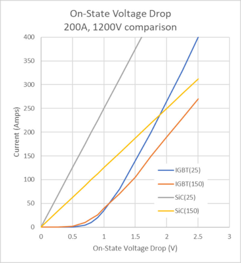
Figure 1a compares the on-state characteristics of an ON Semiconductor FET with a standard 200A, 1200V IGBT. For all operating conditions below 200A, the use of SiC semiconductors can reduce conduction losses, especially in the absence of knee voltage.
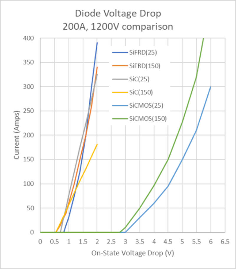
Figure 1b compares the third quadrant characteristics of a Si FRD (First Recovery Diode), an ON Semiconductor FET, and a SiC MOSFET without the use of an anti-parallel Si FRD or a Schottky diode in the SiC semiconductor. If the SiC MOSFET does not have an anti-parallel diode or a SiC Schottky diode integrated, the conduction losses of the SiC MOSFET are much higher than the conduction losses of the FRDs commonly used with IGBTs. Both SiC MOSFETs and Cascode FETs operate at low QRR (often 10 times lower than Si FRDs). Thus, while SiC FETs can switch much faster than IGBTs, synchronous rectification is essential to avoid excessive third quadrant conduction losses.
SiC diodes are widely used in PFC circuits and boost converters. This is because EON losses in low-side FETs are greatly reduced because SiC diodes have no stored charge, whether in 650V superjunction MOSFETs at 400V bus voltages or fast IGBTs at 600-1500V bus voltages. is. In fact, the advantage of using SiC JBS diodes increases with voltage. Even without using SiC FETs as the main switching device, these diodes contribute to increased efficiency and higher operating frequencies. The market size for these products is still over 10 billion yen ($100 million).
Advantages of SiC semiconductors in hard-switched circuits
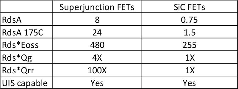
Table 1 shows the datasheet parameters required when evaluating a switch technology for a hard switching application. Let's look at some key points:
For server power supplies, telecom rectifiers operating at 400V bus voltage and on-board chargers, totem pole PFC topologies or 3-phase active front-end rectifiers are used depending on the power level. To improve power density and reduce BOM cost, higher switching frequencies are required to reduce the inductor size. The high EON losses of the high-side FETs prevent the use of superjunction FETs in continuous conduction mode (CCM).
Due to excessive losses and recovery characteristics, lowering the breakdown voltage to reduce QRR will result in poorer lifetime. ON Semiconductor's SiC cascode JFET solutions use diodes with excellent low QRR characteristics, resulting in significantly reduced EON losses. Available in Kelvin source packages such as TO247-4L, D2PAK-7L and DFN8x8, designers can achieve hard switching frequencies 2-3x higher than can be achieved with silicon. All ON Semiconductor SiC cascode JFET products also offer optional low TCR (temperature coefficient of resistance) characteristics. Using low TCR products reduces the increase in on-resistance with temperature.
Advantages of SiC Semiconductors in Soft Switch Circuits
Phase-shifted full-bridge and LLC circuits for DC-DC conversion are widely used in server power supplies and telecom rectifiers, as well as EV on-board chargers and DC-DC converters. The value of wide bandgap switches in general, and SiC-based FETs in particular, in these applications stems from several key characteristics:
First, SiC cascode JFETs have a lower Coss, which allows for a faster VDS transition at turn-on, enabling the use of higher switching frequencies or wider input/output voltage ranges.
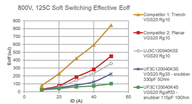
Second, the turn-off losses due to soft switching can be estimated as the measured hard-switching turn-off energy minus the energy stored in the output capacitance, denoted as EOFF-EOSS, and SiC cascode JFETs such as ON Semiconductor's UF3C120040K4S have very low turn-off energy, as shown in Figure 2.
Third, the low RDS(ON) values combined with high voltage ratings enable operation of the DC-DC converters at 800V.
Fourth, SiC cascode JFETs have extremely high voltage slew rates in the range of 100-200 V/ns and small reverse recovery charge characteristics, which virtually eliminates dv/dt induced disturbances without shortening carrier lifetimes.
Finally, ON Semiconductor's SiC cascode JFETs in particular have a very low body diode voltage drop of typically 1.5 V compared to 3-5 V for SiC MOSFETs and GaN HEMTs. As frequency increases, the percentage of time that the body diode conducts increases, resulting in even greater diode conduction losses during dead time.

A loss of 100µJ at 50A, 800V means that the device develops turn-off switching losses of 10W at 100kHz when used in a PSFB at that current. At low currents, these low losses allow frequencies up to 500kHz
Advantages of SiC Semiconductors in EV Traction Inverters
The low losses of ON Semiconductor's SiC cascode JFETs in hard switching provide advantages for EV traction inverters, as well as lower electromotive conduction losses at lower operating frequencies in motor drives.
This is already shown in Figures 1a and 1b. This is due to the low resistance per unit chip area and, unlike IGBTs, the absence of knee voltages in forward conduction as well as the possibility of reverse conduction due to synchronous rectification. An important characteristic of the switches required for EV applications is to withstand various types of short circuit faults. This requires that the switch must withstand the entire bus voltage (650V devices in the case of 400V, 1200V devices in the case of 800V) and at the same time withstand the large current that flows. This large current flows when the gate is fully on, which is 0.5-2µs after the blanking time, and must flow for 2-6µs, until the desaturation detection circuit finds the short circuit condition.
The driver then tries to turn the switch off quickly. During this time, the temperature rise of the switch can be 300-500°C in a few µs, but it still needs to be turned off safely. Furthermore, the switch needs to handle up to 100 or 1000 such events without shifting the device parameters. This characteristic is met for IGBTs, but SiC MOSFETs and GaN HEMTs struggle to meet the same level of robustness. ON Semiconductor's SiC cascode JFETs offer the ability to safely handle repeated short circuits while minimizing the trade-off in chip size or on-resistance. This is due to the inherent properties of normally-on JFETs, which are bulk conduction devices, have no gate oxide to degrade, and can withstand higher temperatures and electric field peaks than SiC MOSFETs.
Additionally, the reduction in channel conductance due to self-heating causes the device to rapidly reduce current and heat up slower, allowing the device to last longer before failing. SiC devices are generally more robust in this mode because these vertical devices absorb the heat within their volume, whereas GaN HEMTs are lateral devices that generate heat in an ultrathin 2D electron gas.
Advantages of SiC Semiconductors in Linear Mode Applications
Figure 3 shows the normalized VTH vs. temperature characteristics of a normally-on SiC JFET, a SiC MOSFET, and a Si MOSFET. It is clear that only the normally-on SiC JFET avoids the degradation of VTH with temperature.
If the device is used as a current source or in a solid-state breaker that is deliberately switched slowly, even in the low current, low |VGS-VTH| region, depending on the time spent, the device may be susceptible to current filamentation and have a negative VTH temperature coefficient, resulting in failure at a much lower voltage than expected. This has been demonstrated not to happen with ON Semiconductor's SSiC cascode JFETs. Therefore, ON Semiconductor's SiC cascode JFETs are very useful for forming current sources, electronic loads, etc. They can be biased in the low current, high voltage loss region without breaking down all the way up to their rated breakdown voltage.
Negative slopes result in unstable operation at high VDS and low |VGS-VTH|. This problem does not exist in normally-on SiCJFETs.
Advantages of SiC semiconductors in circuit protection
The fact that VTH does not degrade with temperature, the excellent current limiting and shorting capabilities of SiC JFETs, and the ability of SiC JFET devices to withstand four times higher energy dissipation than silicon devices to failure, make these devices a circuit breaker, Very useful as an inrush current limiter and load switch. JFETs offer the lowest RDS(ON) for a given chip size and can withstand repeated overstress events, thus reducing conduction losses during operation without compromising device robustness.
A New Approach to Flexible High Voltage FETs
ON Semiconductor has implemented the Super-Cascode approach to high voltage FETs. This is a very high voltage switch realized by connecting many normally-on JFETs in series using low voltage Si MOSFETs and a proprietary bias network. This product can be used as a three terminal switch in composite devices. A 200A, 6500V half bridge module under development has five stages of 1700V JFETs connected in series. The device can be switched with a single gate drive from 0 to 12V with low Qg.
There is no need to provide gate drives for each stage as would be required for series connected IGBTs or SiC MOSFETs. In another demonstration of a low current switch, the Super Cascode technology was applied to a 40kV single switch. The maturity of low voltage JFET technology and low material cost allows designers to offer previously unattainable low cost solutions for higher voltages. Also, when devices are not available for the desired voltage or current class, they can be easily built using ON Semiconductor Cascode and JFET devices.
This article has attempted to cover a lot of the bases while briefly explaining the benefits of ON Semiconductor's SiC cascode JFETs and SiC JFET-based solutions for a wide range of applications - for more detailed information on these subjects please refer to the ON Semiconductor website and publications.
ON Semiconductor's SiC cascode JFETs can not only improve the design of high frequency DC-DC and AC-DC applications, but also allow a drop-in replacement for existing silicon-based designs due to their wide gate drive operating range. The advantages of ON Semiconductor's SiC cascode JFETs in EV inverters have been explained, from low conduction losses to robust short circuit handling. Active mode and circuit protection applications, especially for high voltage and high power, are areas unique to SiC JFET technology, where low voltage JFETs can be used as building blocks to build flexible high voltage, high current switches. These applications have already been discussed in other articles published. Please refer to them as well.
Inquiry
If you have any questions regarding this article, please contact us below.
On Semiconductor Manufacturer Information Top Page
If you want to go back to ONSEMI maker information top page, please click below.