
![]()
![]() Narrow down by specifying conditions
Narrow down by specifying conditions
現在1888件がヒットしています。check
What are the points to keep in mind when selecting an ESD protection device? !
For those who have trouble with device damage or electronic device malfunction due to static electricity, we will introduce selection methods and characteristics to be aware of for ESD protection elements that protect devices from ESD that enters electronic devices.
The following points should be noted when selecting an ESD protection device.
- About terminal capacitance of protective element
- About each voltage of the ESD protection element
- About unidirectional or bidirectional
- About Placement and Layout
These four points are explained in detail below.
1. Capacitance between terminals of protective element
Since the ESD protection diode is inserted between the signal line and GND, the capacitance between the diode terminals may affect the signal line when the protection function is not working.
Therefore, especially when used for high-speed data lines,
- Select a protective element with a small terminal capacitance.
- Low insertion loss for high frequencies
- No problem with eye pattern
must be confirmed.
2. Each voltage of the ESD protection element
There are three voltage values listed in the datasheets of ESD protection devices that you should pay attention to when making a selection.
- Reverse Working Voltage (Peak Reverse Working Voltage): VRWM
- Reverse breakdown voltage (reverse breakdown voltage): VBR
- Clamp voltage: Vc
Points to note for each voltage are described below.
Reverse working voltage: VRWM
At this voltage, the ESD diode, as a high-impedance element, conducts very low leakage currents and thus appears to be in an "off" state.
VRWM is less than the reverse breakdown voltage VBR.
Reverse breakdown voltage: VBR
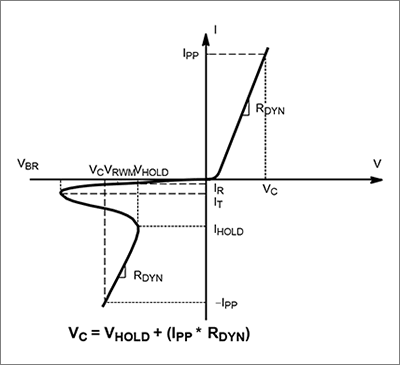
At this voltage the ESD diode begins to conduct, or turn "on".
The breakdown voltage is measured at the test current IT. VBR is specified at the minimum value for ESD applications and is typically 10-15% higher than VRWM.
When choosing an ESD protection diode, ensure that this voltage is higher than the maximum operating voltage of the system to be protected.
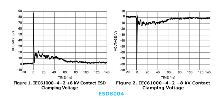
Clamp voltage: Vc
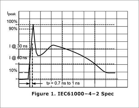
The typical ESD standard at the system level is IEC61000-4-2, identified by sub-nanosecond rise times and high current level waveforms as shown in the figure to the right.
An ESD protection device not only can withstand this ESD stress, but also keeps the voltage applied to the circuit element it protects very low during an ESD event so that subsequent circuit elements it protects can survive. is also necessary.
The clamp voltage is the voltage drop across the ESD protection diodes during an ESD event.
Keeping this clamp voltage low reduces the voltage value to which the circuit element in the subsequent stage to be protected is exposed, and the residual current to the circuit element in the subsequent stage can be suppressed. Therefore, for sensitive circuits such as high-speed lines, it is important to keep this clamping voltage as low as possible.
3. About unidirectional or bidirectional
When selecting an ESD protection device, check the following points regarding whether to select a unidirectional type or a bidirectional type.
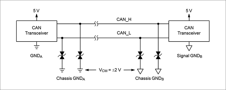
Generally, a unidirectional type is selected, but in cases such as antenna line protection, the electrical signal oscillates in the + and - sides. In such cases, use bidirectional types.
Also, in systems that use a common ground and have multiple remote modules connected through long cables, such as the CAN system in the figure below, the common-mode voltage specification may be reduced if there is a large potential difference between the ground references of the transmitting and receiving nodes. is stipulated.
Prevents clamping of protection devices when a data line offset (the voltage on the data line plus a few volts positive or negative offset to its nominal voltage level) occurs within the specified common-mode range must use bidirectional types.
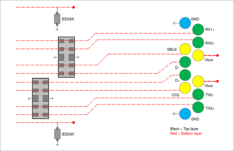
4. Placement and layout
Place the ESD protection diode as close to the noise source as possible, such as a connector, minimize the parasitic inductance of the PCB, and minimize the loop area formed by the high-speed data line and ground line. is asked.
Therefore, by using ESD protection element products compatible with each interface, wiring pattern design becomes easier. There are also products that protect multiple lines with a single chip, so costs and board space can be reduced when compared to discrete designs.
<Layout for USB 3.1 Type-C>
Reference: ON Semiconductor Application Note
Maintaining Signal Integrity When Selecting ESD Protection for USB 3.0 Interfaces [AND9114JP/D]
How to Maintain USB Signal Integrity When Adding ESD Protection [AND8319JP/D]
An Overview of High-Speed Digital Signal Analysis Using the Data Eye Diagram Technique [AND9075JP/D]
Interpreting datasheet parameters for ESD devices [AND8308JP/D]
Characterization of ESD Clamp Performance [AND8307JP/D]
PCB Design Guidelines for Maximizing TVS Diode Performance [AND8232JP/D]
Application Tips for Transient Voltage Suppression Diode Circuits [AND8230JP/D]
For those who want to know more about ESD protection devices
This article introduced points to consider when selecting an ESD protection device. If you would like to know more about the content of the article or ESD protection diodes, please feel free to contact us below.
Click here for manufacturer site/other related links
Onsemi Manufacturer information Top
If you want to go back to ONSEMI Manufacturer Information Top, please click below.