
![]()
![]() Narrow down by specifying conditions
Narrow down by specifying conditions
現在1888件がヒットしています。check
Introduction
In recent years, as the resolution of cameras has increased, the performance of CMOS sensors used as image sensors has improved dramatically, and the output interface of CMOS sensors has changed along with the increase in the amount of video transmission data to be handled.
While the adoption of MIPI I/F output CMOS sensors is progressing in a wide range of fields such as digital cameras, single-lens reflex cameras, professional camcorders, medical cameras, in-vehicle cameras, and FA cameras, SoCs and CPUs connected to CMOS sensors are becoming increasingly popular. There are many cases where MIPI I/F is not supported or MIPI ports are insufficient.
Professional camcorders and single-lens reflex cameras are equipped with sub-monitors, rear displays, and electronic viewfinders, and the displays used in these are also increasingly compatible with MIPI I/F, and these are also SoCs and CPUs. Direct connection is not possible because it is not compatible with the interface with.
For these reasons, in products that handle CMOS sensors and displays, there is an increasing need for interface conversion between CMOS sensors and SoCs, and between SoCs and displays, as shown in the figure below.
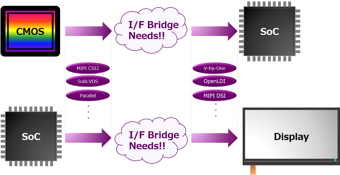
Interface conversion using FPGA is convenient when such interface conversion is necessary.
In particular, Lattice FPGA has a wide range of devices that specialize in mutual interface conversion on the CMOS sensor and display side, centered on MIPI I/F, and has many solutions that take advantage of the flexibility unique to FPGA. On this page, we will introduce examples of Lattice FPGA utilization mainly for interface conversion.
In this article, we will pick up and introduce the following four cases.
1. I want to connect multiple CMOS sensors
2. I want to implement interface conversion + image processing
3. Want to process multiple video signals in parallel
4. I want to perform high-speed communication while suppressing power consumption
1. I want to connect multiple CMOS sensors
In the case of compound eye cameras, which have been increasing in recent years, there are many cases where CMOS sensors cannot be directly connected because the SoC and CPU that perform image processing do not have multiple MIPI ports. As shown in the figure below, Lattice FPGA can implement an aggregation function that bundles multiple MIPI I/F channels into one MIPI I/F channel, making it possible to connect multiple CMOS sensors. Each CMOS sensor can be identified by VC (virtual channel) information.
Lattice FPGA also has devices that can support up to the industry's fastest MIPI I/F Max 2.5Gbps/lane, so it is possible to connect multiple high-resolution CMOS sensors and perform MIPI I/F aggregation. increase.
Also, since there are FPGAs with DSP and DDR memory interfaces, it is possible to reduce the load on the subsequent SoC and CPU by implementing the image processing function at the same time as MIPI I/F aggregation as shown in the figure below.
*The yellow part of the block below is the Lattice FPGA.
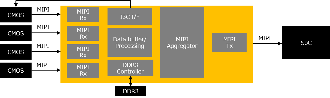
(1) Configuration example of MIPI I/F aggregation using Lattice FPGA
2. I want to implement interface conversion + image processing
It is a case of not only converting the interface from the CMOS sensor, but also realizing image processing at the same time.
The case where image processing is realized at the same time as interface conversion was touched on in Section 1, but this example is a case where image processing is the main, and all the image processing functions realized by SoC and CPU are incorporated into FPGA, It will be a solution to reduce the number of chips.
In the case of Lattice FPGA, it is possible to propose a small package + low power consumption FPGA in the case of realizing image processing at the same time as interface conversion.
In addition to clock parallel interfaces such as LVDS, Sub-LVDS, and SLVS, we also have FPGAs that are compatible with clock-embedded high-speed transmission interfaces, making it possible to make proposals in a wide range of fields.
*The yellow part of the block below is the Lattice FPGA.
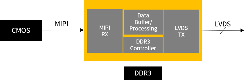
(2) Configuration example of interface conversion + image processing by Lattice FPGA
3. Want to process multiple video signals in parallel
As shown in the figure below, video signals input from two CMOS sensors are split inside the FPGA, one channel is input to the subsequent SoC, and the other channel is connected to the display. It can be converted and processed.
In some cases, dedicated chips are used for interface conversion, but FPGAs are the best way to achieve such parallel conversion and processing of multiple systems on a single chip.
Even if the specification of the SoC changes or the specification of the connected display changes, it is possible to flexibly respond by simply changing the internal circuit of the FPGA without having to make a large-scale board revision if it is an FPGA. is.
In the case of Lattice FPGA, many reference designs and IPs for MIPI I/F and other interfaces Rx and Tx have been released. I have.
*The yellow part of the block below is the Lattice FPGA.
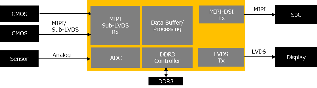
(3) Configuration example of parallel processing of multiple video signals by Lattice FPGA
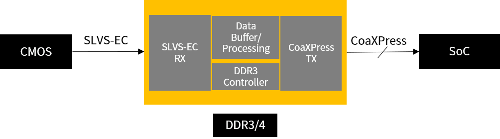
4. I want to perform high-speed communication while suppressing power consumption
Lattice is constantly developing new FPGAs called the NX series that employ a process called FD-SOI, and it is possible to achieve low heat generation while performing high-speed communication of video/image system I/F SLVS-EC and CoaXPress.
As shown in the figure below, the video signal input from the CMOS sensor is processed inside the FPGA and input to the subsequent SoC, enabling high-speed communication and data processing of up to 10 Gbps with low power consumption.
Even if there are changes in SoC specifications, availability, etc., and changes in CMOS sensor specifications due to functional upgrades, FPGAs do not require large-scale board revisions. It is possible to respond flexibly.
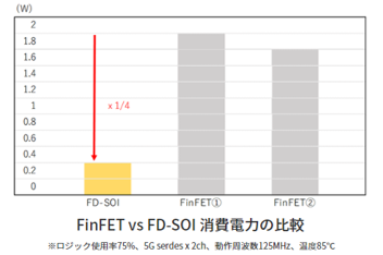
In addition, when comparing the power consumption of other companies' FinFETs under the same conditions, it is possible to achieve low power consumption of about 1/4.
*The yellow part of the block below is the Lattice FPGA.
④High-speed communication configuration example and power consumption comparison by Lattice FPGA
Document download
For those who want to know the specific product names and package lineup that can realize these solutions, detailed information is provided in the following materials. As mentioned at the beginning, the example introduced in this article is an example, and there are various other solutions. Please take a look at it!
With Japanese manual! Free MIPI CSI-2 reference design now available!
We have created Macnica 's original MIPI CSI-2 reference design.
You can download it for free by clicking the button below.
In addition, MIPI DSI and SERDES reference designs are also available.
For details, please check here.
▼▽▼▽▼▽▼▽▼▽▼▽▼
Inquiry
If you have any questions regarding this article, please contact us below.