- Semiconductor BusinessHOME
- Products and Services of Macnica,Inc.
-
technical information

-
Events and Seminars
- Handling Manufacturer
- Support
- Inquiry
- Click here to purchase products
- Semiconductor business e-mail magazine registration
![]()
![]() Narrow down by specifying conditions
Narrow down by specifying conditions
現在2182件がヒットしています。check

Part 3: Design and verification of USB 3.0
≪Contents≫
|
 |
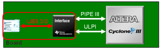
<<USB 3.0 interface design>>
The USB 3.0 interface is divided into two lines, one used in SupreSpeed mode and the other used in Legacy Speed mode. In Legacy Speed mode, it communicates at a maximum of 480 Mbps, and in SupreSpeed mode, it operates at 5Gbps. Therefore, the design of the line used in this SS mode seems to be a bottleneck, but in fact, this part was not so much a bottleneck.
First, SS Line, which communicates at 5 Gbps, is very similar to PCI-Express Gen 2 not only in bandwidth but also in protocol. I referred to the following books for wiring restrictions.

As for other wiring lengths, a reference design has been published by the USB I/F. The wiring length between the PHY and the connector is FR4, 1 to 6 inches (on the device side), and the wiring impedance is 90Ω. , the TI datasheet describes the wiring error of each differential signal within 2.5mil and the recommended capacitors to be used for AC coupling, so the SS Line design can be done easily as mentioned above.
The figure below is a layout diagram of the USB 3.0 Line of the Cyclone® III USB 3.0 Board developed by our company.

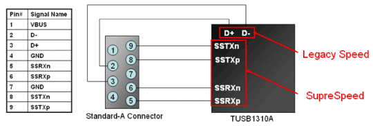
Also, the Cyclone III USB 3.0 Board uses a Standard-A connector so that both sides of the host device can be verified. As some of you may have noticed, the SSRX polarity is reversed. This is intentionally reversed to avoid USB 3.0 crosstalk, but USB 3.0 supports polarity reversal, so there is no problem.
Also, please refer to the diagram below for connections when using the Standard-B connector.

In this way, the design between the PHY and the connector is relatively easy because there is a reference design and the details are determined by the standard.
≪PIPE III interface design≫
Actually, in Cyclone III USB 3.0 Board, designing between FPGA ⇔ PHY was more difficult than designing between PHY ⇔ connector. FPGA ⇔ PHY are connected by PIPE III interface and ULPI interface. PIPE III (for SS mode) interface has 125 MHz SDR x32 bit, 250 MHz SDR x16 bit and 500 MHz SDR x8 bit. This time it became a 250 MHz SDR x16 bit interface. The ULPI interface (HS, FS, LS mode) is 60 MHz SDR x8 bit, so design is relatively easy, but on top of the above 250 MHz SDR, it is a parallel bus, and the board design is detailed according to the standard. The biggest challenge this time was that it hadn't been decided yet, and of course, this was the first time for us to design PIPE III, so we proceeded with the design carefully.

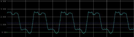
First, we perform topology verification of PIPE III. From TI's datasheet, TX_DATA, TX_DATAK, RX_DATA, RX_DATAK, and PCLK are 250MHz SDR signals and are the most sensitive lines in PIPE III. As I mentioned last time, the transmission simulation is the most reliable for designing without a proven track record. We used HyperLynx® again this time to perform IBIS simulations and determine the topology of PIPE III.
Therefore, this time, we will introduce how we verified TX_DATA and TX_DATAK of the PIPE III interface. Also, the above signals are output signals from the FPGA to the PHY.
First, when we verified a topology without a damping resistor between the FPGA and PHY, ringing was seen near the threshold in terms of signal quality, which left us with uneasy results.

When it comes to equal length wiring, the board design becomes quite complicated.

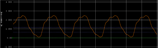
Next, I verified a pattern that uses FPGA internal resistors for the TX_DATA and TX_DATAK lines. The signal quality was better than when the external resistor was installed, and although there was a crack in the signal, the threshold had some margin, so the waveform was relatively satisfactory. Considering board design, we decided on a topology that uses internal resistors.


In this way, I proceeded with the board design and was able to confirm the operation in one try without actually remaking the board! !
As for what kind of environment we are actually conducting the operation verification, we connected it to the PC with the USB 3.0 interface, made the PC recognize the DDR2 memory installed in the Cyclone III USB 3.0 Board as a RAM disk, and benchmarked it. is a method of measuring (In a nutshell, use it as USB 3.0 mass storage class and do a benchmark measurement)
The tool used for benchmark measurement is "CrystalDiskMark". Currently, it operates at about 210MB/s for Read and about 180MB/s for Write (as of August 30, 2010). As a USB 3.0 mass storage class, it's a good result. (The driver uses the Windows default driver, not a special one!)
I would love to see the demo of the mass storage class above! ! Please feel free to contact us if you say.
Thank you very much for reading this article three times. I would appreciate it if you could help me with your design.
Part 1: Realization of USB 3.0 interface using FPGA
Part 2: How to verify the design of DDR 2?