- 半導体事業HOME
- マクニカの製品・サービス
-
技術情報

-
イベント・セミナー
- 取扱メーカー
- サポート
- お問い合わせ
- 製品購入はこちら
- 半導体事業のメルマガ登録
![]()
![]() 条件を指定して絞り込む
条件を指定して絞り込む
現在2189件がヒットしています。check

第1回 FPGAを使用して USB 3.0 インタフェースの実現
≪目次≫
|
|
≪USB 3.0 ソリューションの概要≫
USB 3.0 とは、PC 周辺機器を接続するためのインタフェースなどで広く使われている USB の次世代規格です。また、「Super Speed モード」とも呼ばれており、従来の 「High Speed モード(USB 2.0)」 の通信速度 (480 Mbps) の10倍以上となる5 Gbps という高速データ通信が可能になっています。また、USB 3.0 は下位互換を持っており、従来の 「High Speed モード」、「Full Speed モード (USB 1.1/12 Mbps)」、「Low Speed モード (USB 1.0/1.5Mbps)」 用の USB 製品もそのまま使用することができます。
近年、データが大容量化してきており、その大容量のデータをいかに高速に転送するかが問題になってきている中で 「USB 3.0 での5Gbps 通信」 というのは、今後市場で動向が期待されています。
≪FPGA を使用して、USB 3.0 インタフェースの実現≫
ASSP や ASIC などを使用して USB 3.0 インタフェースを実現することも可能です。しかし ASSP だと機能に制限があり、汎用性にかける部分があります。また、ASIC だと開発期間・高リスクなどの大きな課題があります。
そこで弊社は、アルテラ社 FPGA を使用して USB 3.0 インタフェースの実現をご提案いたします。FPGA を使用することにより、デバイス内部のデザインをユーザの仕様に合わせて書き換えが出来るので、ASSP での課題であった汎用性が解決され、ASIC の課題であった開発期間・高リスクなどの課題も大幅に改善されます。
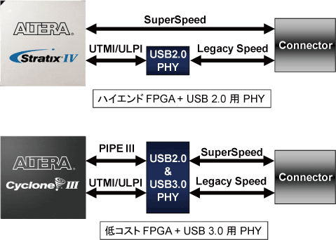
アルテラ社 FPGA を使用して USB 3.0 インタフェースの実現方法として、大きく分けて2通りあります(Fig. 1 参照)。まず、5Gbps 以上のトランシーバを内蔵している、FPGA を使用する方法です。この方法では「Super Speed モード」のトランシーバ役は FPGA が行いますので、USB 3.0 インタフェース用の外付け PHY を用意する必要がありません。しかし USB 2.0 インタフェース用の外付け PHY を用意する必要があります。PIPE III インタフェースを基板上で接続する必要がないので、基板設計は楽になると言うメリットはあるものの、現在 5Gbps 上のトランシーバ内臓 FPGA となると、ハイエンド FPGA に含まれるものがほとんどであり、コスト面で量産には向かないと言うデメリットがあります。
次に、低コスト FPGA と、USB 3.0 インタフェース用の外付け PHY を使用する方法です。PIPE III インタフェースを基板上で接続する必要があるので、基板面積・配線数などが増えるデメリットはありますが、上記で述べたハイエンド FPGA を使用する方法に比べるとコスト面が抑えられ量産には向いていると言えます。
≪低コスト FPGA を使用した USB 3.0 Board≫
「新規格はコスト面も実績面も不安」 と思われるでしょう。実際に何の実績もない中、どれだけご提案しても、絵に画いた餅になります。そこで弊社はこの度、実機レベルで USB 3.0 インタフェースを低コストのソリューションとしてご提案できるように、低コスト FPGA を使用した USB 3.0 インタフェースを実現する基板を製作しました。
基板には、DDR2 / MRAM / HSMC ・・・・ などの USB 3.0 以外のソリューションを仕様に盛り込むことで、拡張性に優れ様々なケースに合わせて検証できる仕様になっております(基板のブロック図は “Fig.2” 通りになります)。
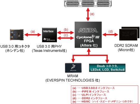
Fig. 2
また、USB 3.0 インタフェースを実現する基板製作にあたって、USB 3.0 用の PHY は、Texas Instruments 社の TUSB1310、FPGA にプログラミングする USB 3.0 用の IP としてインベンチュア社の IP、USB 3.0 用コネクタ/ケーブルにホシデン社にご協力いただきました。
次回はこの基板にも搭載されたメモリインタフェースとしてよく使用されている DDR 2 インタフェースのご紹介をいたします。ボード設計に失敗しない使えるヒントが満載です!また最終回はこの基板を使用した、USB 3.0 ソリューションをご紹介いたします。あの次世代インタフェースが低コストで実現できた秘密を公開します。