- Semiconductor BusinessHOME
- Products and Services of Macnica,Inc.
-
technical information

-
Events and Seminars
- Handling Manufacturer
- Support
- Inquiry
- Click here to purchase products
- Semiconductor business e-mail magazine registration
![]()
![]() Narrow down by specifying conditions
Narrow down by specifying conditions
現在2183件がヒットしています。check

An easy-to-understand explanation of the appeal of Intel® MAX ® 10 FPGAs. For more detailed information, please refer to Intel's handbook.
 |
Intel's MAX 10 FPGA is a non-volatile FPGA that has significantly improved speed and integration by adopting a process that is more than two generations smaller than CPLD. |
Features
Functions implemented in hardware
![]() Configuration memory
Configuration memory
The FPGA loses its configuration image when the power is turned off. The MAX 10 FPGA automatically transfers the configuration image stored in the flash memory to the FPGA every time the power is turned on.
- Built-in flash memory for configuration eliminates the need for an external configuration memory.
- When the power is turned on, it starts working within a few milliseconds (instant-on).
- The configuration image is not lost when power is removed (non-volatile).
- Since the flash process is used, reprogramming (erase and write) to the flash memory can be performed up to 10,000 times.
- The area that can be used by the user for purposes other than configuration (UFM (User Flash Memory))) is up to 736Kb.
- Stores two configuration images (dual configuration) and you can switch them dynamically (on the fly).
<Usage examples that make the most of the features>
- Place the factory configuration image in one area and the new image during a system upgrade in the other area. If there is a problem after the upgrade, you can switch to the factory state (fail-safe upgrade function).
- Using a configuration time (a few ms) that is significantly shorter than the time it takes a human to press a button (a few hundred ms), you can switch between two functions with each button press. (There is no limit on the number of times the flash memory can be read).
![]() LE (logic element)
LE (logic element)
- A MAX 10 FPGA has up to 50,000 LEs. Since the maximum number of LEs of MAX V CPLD is 2,210, it is about 23 times larger.
LE is a part of FPGA to make logic circuit. If you use this, you can also make a processor, so you can make a high-performance microcomputer.
- It has a 12-bit, 1Msps (million samples per second) ADC (Analog-to-Digital Converter) with up to 18-channel input and a TSD (Temperature Sensing Diode) for correction.
Analog signals from voice and various sensors can be converted to digital signals by ADC and then processed digitally.
![]() internal memory
internal memory
- It has up to 1.6Mb of SRAM.
- As mentioned in the configuration memory section, UFM is also available up to 736Kb.
![]() DSP (Digital Signal Processor) block
DSP (Digital Signal Processor) block
- Equipped with a DSP that can configure up to 144 18x18 multipliers and up to 288 9x9 multipliers.
Multipliers can also be made with LEs, but a single 18x18 multiplier uses hundreds of LEs. Therefore, if you use the optimized parts "DSP" to make a multiplier, you can make a multiplier faster than LE without using LE.
![]() oscillator
oscillator
- It has an internal oscillator that generates a clock signal.
It works just by turning on the power, so it can be used for watchdog timers and sleep controllers.
![]() global clock line
global clock line
- It has up to 20 global clock lines.
A global clock line is a low-delay and low-skew routing that connects directly to each cell, such as an LE or DSP.
Use for clocks and reset signals with high fanout (connected to many cells such as LEs).
![]() PLL (Phase Locked Loop)
PLL (Phase Locked Loop)
- Equipped with up to four PLLs that divide/multiply the clock signal and match the phase.
The PLL can generate 10 stable internal clocks with different frequencies and 2 external clock signals from a single clock signal.
![]() AES (Advanced Encryption Standard)
AES (Advanced Encryption Standard)
- Since the flash memory and FPGA are mounted on a single chip, the product is structurally stronger in security than placing the flash memory externally. AES.
![]() I/O
I/O
- Supports 3.3V, LVDS, mini-LVDS, PCI and over 30 I/Os as standard.
![]() EMIF (external memory interface)
EMIF (external memory interface)
- You can use the controller provided with the IP to interface with externally located memory such as SRAM, DDR2/3 and LPDDR2.
![]() voltage regulator
voltage regulator
- There are products that supply dual power supplies of 2.5V and 1.2V and single supply products of 3.3V (or 3V).
Single-supply products have integrated regulators that generate the 2.5V and 1.2V supplies required by the FPGA core, reducing the number of external power devices required. Dual power products require two power supplies but offer better performance.
Other features and packages
![]() sleep mode
sleep mode
- It supports a sleep mode that turns off clocks and I/Os when no activity is needed, saving up to 95% power.
![]() Dynamic Input Buffer Disable Feature
Dynamic Input Buffer Disable Feature
- The input buffer portion of the bi-directional buffer can be automatically turned off during operation without reconfiguring (reconfiguring) the FPGA.
This allows for dynamic (during operation) power down when the input buffer is not needed, for example during DDR3 idle or writes. In the case of LVDS, the user can control ON/OFF.
- The increase in the number and speed of LEs has made it possible to install the 32-bit soft-core processor Nios II.
Unlike microcomputers, Nios II peripherals can be freely created using LE.
![]() package
package
- 3mm useful for space constrained systems 2 from WLCSP (Wafer Level Chip Size Package)
Available in FBGA packages with up to 500 user I/Os.
Product and package list
Product Line
| 10M02 | 10M04 | 10M08 | 10M16 | 10M25 | 10M40 | 10M50 | |
| Number of LEs (Logic Elements) | 2,000 | 4,000 | 8,000 | 16,000 | 25,000 | 40,000 | 50,000 |
| Internal memory (SRAM) (Kb) | 108 | 189 | 378 | 549 | 675 | 1,260 | 1,638 |
| UFM (User Flash Memory) (Kb) | 12 | 16–156 | 32–172 | 32–296 | 32–400 | 64–736 | 64–736 |
| Number of DSPs (18x18 bit multipliers) | 16 | 20 | 24 | 45 | 55 | 125 | 144 |
| Number of PLLs | 1 or 2 | 1 or 2 | 1 or 2 | 1 or 4 | 1 or 4 | 1 or 4 | 1 or 4 |
| internal configuration | single | dual | dual | dual | dual | dual | dual |
| Number of ADCs/TSDs | - | 1/1 | 1/1 | 1/1 | 2/1 | 2/1 | 2/1 |
| EMIF | ○ | ○ | ○ | ◎ | ◎ | ◎ | ◎ |
Note 1: The number of PLL/ADC/TSD, etc. varies depending on the package type.
Note 2: EMIF ○ ⇒ SRAM
Note 3: ◎ in EMIF ⇒ SRAM, DDR3 SDRAM, DDR2 SDRAM, LPDD
Package List
 |
 |
 |
| WLCSP | MBGA/UBGA/FBGA | EQFP |
| package line | content |
10M02 |
10M04 | 10M08 | 10M16 | 10M25 | 10M40 | 10M50 |
| V36 | WLCSP (3 mm, 0.4 mm pitch) |
○ | - | - | - | - | - | - |
| V81 | WLCSP (4mm, 0.4 mm pitch) |
- | - | ○ | - | - | - | - |
| F256 | FBGA (17mm, 1.0 mm pitch) |
- | ○ | |||||
| U324 | UBGA (15mm, 0.8 mm pitch) |
○ | - | - | - | |||
| F484 | FBGA (23mm, 1.0 mm pitch) |
- | - | ○ | ||||
| F672 | FBGA (27mm, 1.0 mm pitch) |
- | - | - | - | ○ | ||
| E144 | EQFP (22mm, 0.5 mm pitch) |
○ | ○ | ○ | ||||
| M153 | MBGA (8mm, 0.5 mm pitch) |
○ | - | - | - | - | ||
| U169 | UBGA (11mm, 0.8 mm pitch) |
○ | - | - | - | |||
Note: The same ○ is pin compatible.
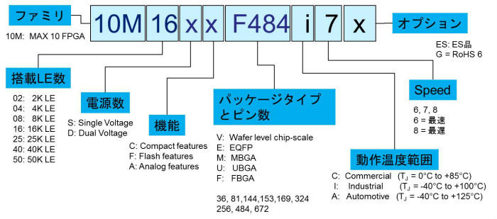
How to read the product code
development kit
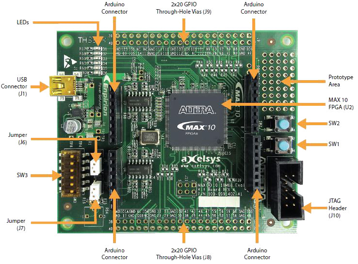
MAX 10 FPGA 10M08 Evaluation Kit
Compact and inexpensive evaluation kit with MAX 10 FPGA 10M08 and 80 I/O through-holes.
 |
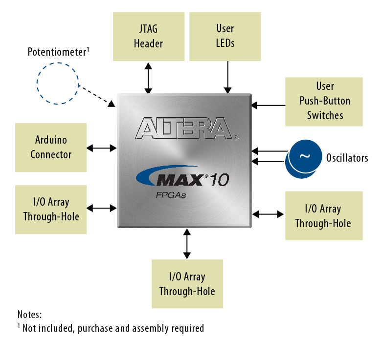 |
| board photo | Block Diagram |
If there is an enlarged image, click on the image to enlarge it.
MAX 10 FPGA 10M50 Evaluation Kit
Evaluation kit featuring MAX 10 FPGA 10M50, Ethernet, HSMC, SPI, DDR3 and more.
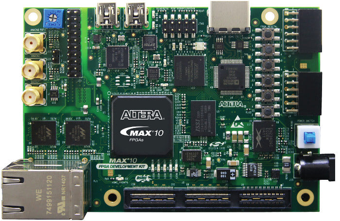 |
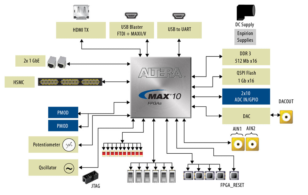 |
| board photo | Block Diagram |
If there is an enlarged image, click on the image to enlarge it.
Q&A
![]() Can I design with the free Quartus ® II Web Edition?
Can I design with the free Quartus ® II Web Edition?
- Yes, you can use the free Quartus ® II Web Edition to design all MAX 10 FPGA products.
![]() I would like to use a product smaller than 2,000 LE?
I would like to use a product smaller than 2,000 LE?
- Take advantage of MAX V CPLDs with 40 to 2,210 LEs. MAX 10 FPGAs are not intended to replace MAX V CPLDs, and MAX V CPLDs will continue to be available.
Related Information
The above specifications are subject to change, so please refer to the following page for the latest specifications.