
![]()
![]() Narrow down by specifying conditions
Narrow down by specifying conditions
現在1888件がヒットしています。check

* This bug has been resolved in the following Quartus Prime. For more information, please see the FAQ below.
・Intel® Quartus® Prime Standard Edition Software v21.1 and later
・Intel® Quartus® Prime Pro Edition Software v21.3 and later
--------------------------------------------------------------------------------------------------------

hello.
My name is Intel F. Hanako and I provide technical support for Intel® FPGA products at Macnica.
A must-see for users using Cyclone ® IV EP4CE75!
Here is a workaround for a bug that occurs when writing a jic file to the configuration ROM via FPGA.
Defect situation
Problems have been confirmed under the following conditions.
| Tools |
Quartus® II 13.1.4 or later (includes Quartus Prime Standard and Lite Editions) |
| FPGA | EP4CE75 |
| File format to transfer | .jic |
| Execution content |
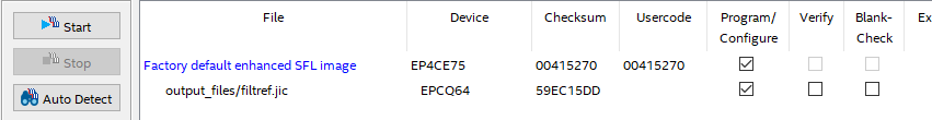
Execute the Program option using the Factory Enhanced SFL image to transfer the jic file to the configuration ROM.
<Programmer GUI image>
|
|
in Programmer Occur Error message |
Error (209025) Can't recognize silicon ID for device … |

Defect factor
There is a bug in the Enhanced Serial Flash Loader (hereafter Enhanced SFL) image for EP4CE75 shipped with Quartus II 13.1.4 and later and Quartus Prime Programmer.
It is not improved in ver.20.1 of Quartus Prime Standard and Lite Editions.
Workaround
Create your own SFL IP for EP4CE75and transfer the jic file to the configuration ROM with the sof file.
The work procedure is as follows.
- Create SFL IP
- Implement SFL IP in top design
- Add timing constraints for your own SFL IP
- compile
- Download sof file to EP4CE75
- Download jic-file
Let's take a look at this work.
1. Create SFL IP
In Quartus Prime, create a new workaround project and select EP4CE75 as the target device.
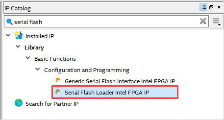
In the Tools menu > IP Catalog, select "Serial Flash Loader Intel FPGA IP".
(When creating with Quartus Prime ver.17.1 or earlier, the IP name is Altera Serial Flash Loader IP.)
Specify an arbitrary name and folder to generate for the IP and enable the following options on the General tab.
Use enhanced mode SFL = On
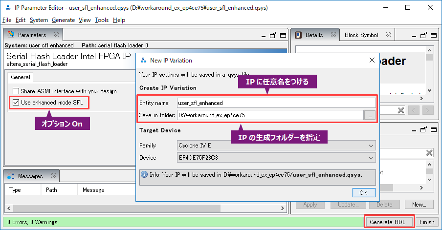
Click the Generate HDL button and specify the language to generate.
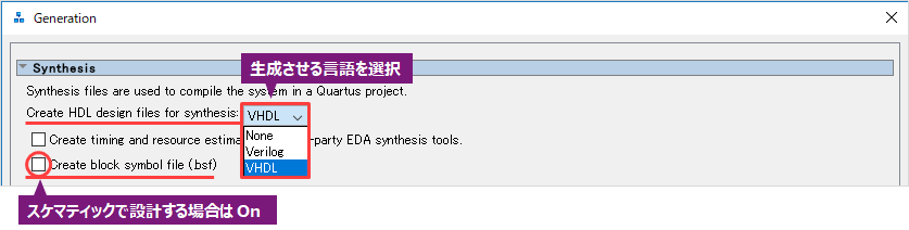
Click the Generate button to generate the SFL IP.
2. Implement SFL IP in top design
Open a blank design file via File menu > New to create a top-level design.
Entity name is arbitrary.
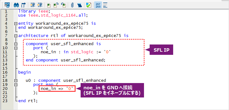
Implement the SFL IP created in step 1 in your top-level design.
(You may find it useful to leverage the templates for instances in the IP's generated folder.)
Connect the input noe_in port to GND to enable the SFL IP.
Below is an example design in VHDL.
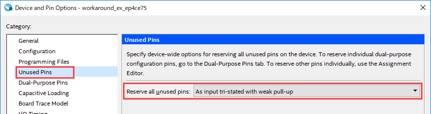
Assignments menu > Device > Device and Pin Options > Unused Pins
Configure unused user I/O pins as follows:
Reserved all unused pins: As input tri-stated with weak pull-up
3. Add timing constraints for your own SFL IP
Create a timing constraint file (.sdc) for the SFL IP.
Please refer to the limitations published on the manufacturer's web page Knowledge Base.
## 参考例 create_clock -name {altera_reserved_tck} -period 100.000 -waveform { 0.000 50.000 } [get_ports {altera_reserved_tck}] create_generated_clock -name {ALTERA_DCLK} -source [get_ports {altera_reserved_tck}] -master_clock {altera_reserved_tck} \ [get_ports {*altserial_flash_loader_component|\GEN_ASMI_TYPE_1:asmi_inst~ALTERA_DCLK}] ## set_input_delay -add_delay -clock [get_clocks {altera_reserved_tck}] 20.000 [get_ports {altera_reserved_tdi}] set_input_delay -add_delay -clock [get_clocks {altera_reserved_tck}] 20.000 [get_ports {altera_reserved_tms}] set_input_delay -add_delay -clock [get_clocks {ALTERA_DCLK}] 11.000 [get_ports \ {*altserial_flash_loader_component|\GEN_ASMI_TYPE_1:asmi_inst~ALTERA_DATA0}] ## set_output_delay -add_delay -clock [get_clocks {altera_reserved_tck}] 20.000 [get_ports {altera_reserved_tdo}] set_output_delay -add_delay -max -clock [get_clocks {ALTERA_DCLK}] 0.000 [get_ports \ {*altserial_flash_loader_component|\GEN_ASMI_TYPE_1:asmi_inst~ALTERA_DCLK}] set_output_delay -add_delay -clock_fall -clock [get_clocks {ALTERA_DCLK}] 0.000 [get_ports \ {*altserial_flash_loader_component|\GEN_ASMI_TYPE_1:asmi_inst~ALTERA_DCLK}] set_output_delay -add_delay -clock [get_clocks {ALTERA_DCLK}] 13.000 [get_ports \ {*altserial_flash_loader_component|\GEN_ASMI_TYPE_1:asmi_inst~ALTERA_SCE}] set_output_delay -add_delay -clock [get_clocks {ALTERA_DCLK}] 8.000 [get_ports \ {*altserial_flash_loader_component|\GEN_ASMI_TYPE_1:asmi_inst~ALTERA_SDO}] ## remove_clock_groups -all ## set_false_path -from [get_ports {altera_reserved_tck}] -through [get_nets \ {*altserial_flash_loader_component|\ENHANCED_PGM:sfl_inst_enhanced|dclkin~0}] -to [get_keepers \ {*altserial_flash_loader_component|\GEN_ASMI_TYPE_1:asmi_inst~ALTERA_DCLK}][Note] The ending number of \GEN_ASMI_TYPE_1may be different.
After creating and saving the sdc file, register the .sdc to the project using the menu below.
Assignments menu > Settings > Timing Analyzer category
4. Compile
Compile.
Processing menu > Start Compilation
5. Download sof file to EP4CE75
Start Programmer. (Tools menu > Programmer)
Set Hardware Setup and select JTAG for Mode.
Set the compiled sof file and enable (On) the Program/Configure option.
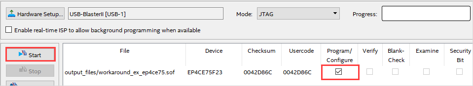
Click the [Start] button to transfer data to the EP4CE75.
After writing is completed, delete the sof file from the Programmer screen using the [Delete] button.
6. Download the jic file
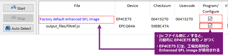
Register the jic file created in advance in the Programmer.
Enable (On) the Program/Configure option in the jic file.
[Reference: Creating a jic file]
Quartus® Guide - Convert Programming Files
Programming to EPCQ devices via FPGA (JIC programming)
Only disable (Off) the Program/Configure option for the Factory default enhanced SFL image.
* By step 5, the SFL image has already been downloaded to EP4CE75.
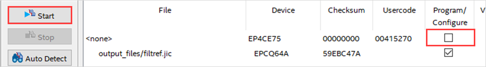
Click the Start button to download only the jic file.
This completes the work.
Please use this method when writing the jic file to the configuration ROM via EP4CE75.
Click here for recommended articles/materials
Intel® FPGA Development Flow/FPGA Top Page
Quartus ® Guide - Convert Programming Files
Programming to EPCQ device via FPGA (JIC programming)