- Semiconductor BusinessHOME
- Products and Services of Macnica,Inc.
-
technical information

-
Events and Seminars
- Handling Manufacturer
- Support
- Inquiry
- Click here to purchase products
- Semiconductor business e-mail magazine registration
![]()
![]() Narrow down by specifying conditions
Narrow down by specifying conditions
現在2182件がヒットしています。check


Introduction
こんにちは。トットです。
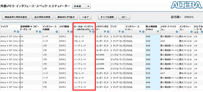
This time, I investigated the local interface clock rate type "half rate" (hereinafter referred to as HDR) described in Spec Estimator. This is the red frame on the screen below.
HDR とは・・・・
HDR is a data transfer method that reduces the frequency by half by making the data width of the local interface four times the data width of the memory interface.
For Intel's FPGA memory interface, DDR3 is controlled by HDR, QDR (Quarter Data Rate).
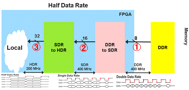
DDR → SDR → HDR
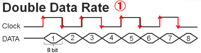
DDR ( Double Data rate )
This is the interface between DDR and FPGA. The memory controller inside the FPGA takes data on the rising and falling edges of the clock.
下図の DATA は各 8 bit です。
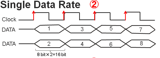
DDR → SDR ( Single Data Rate )
Inside the FPGA, data is passed to the user circuit in two stages. The first step is to convert double rate data to single rate.
Since data is acquired only at the rising edge of the clock, DDR → SDR transfers data in parallel.
1 つデータ幅は 8 bit なので総データ幅は 16 bit になります。
SDR → HDR ( Half Data Rate )
The data that has become single rate in the second stage will also become half rate. Like SDR, data is acquired at the rising edge of the clock, so data is transferred in parallel from SDR to HDR.
However, the difference from SDR is that the operating frequency is halved. By halving the operating frequency, the data width is also twice that of SDR and four times that of DDR.
1 つデータ幅は 8 bit なので総データ幅は 32 bit です。
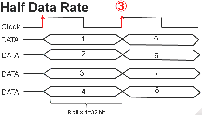
HDR は動作周波数を半分にしても、データ幅を増やすことでデータをとるタイミングは DDR と変わりません。
DDR を HDR にすることで動作周波数が下がり、タイミング設計がしやすくなります。
* QDR のクロック周波数は DDR, SDR の 4 分の 1 でデータ幅は 8 倍です。
今回のまとめ
■HDR transfers data by making the data width of the local interface four times the data width of the memory interface and halving the frequency.
■In the case of Intel's FPGA memory interface, DDR3 is controlled by HDR and QDR.