- Semiconductor BusinessHOME
- Products and Services of Macnica,Inc.
-
technical information

-
Events and Seminars
- Handling Manufacturer
- Support
- Inquiry
- Click here to purchase products
- Semiconductor business e-mail magazine registration
![]()
![]() Narrow down by specifying conditions
Narrow down by specifying conditions
現在2189件がヒットしています。check
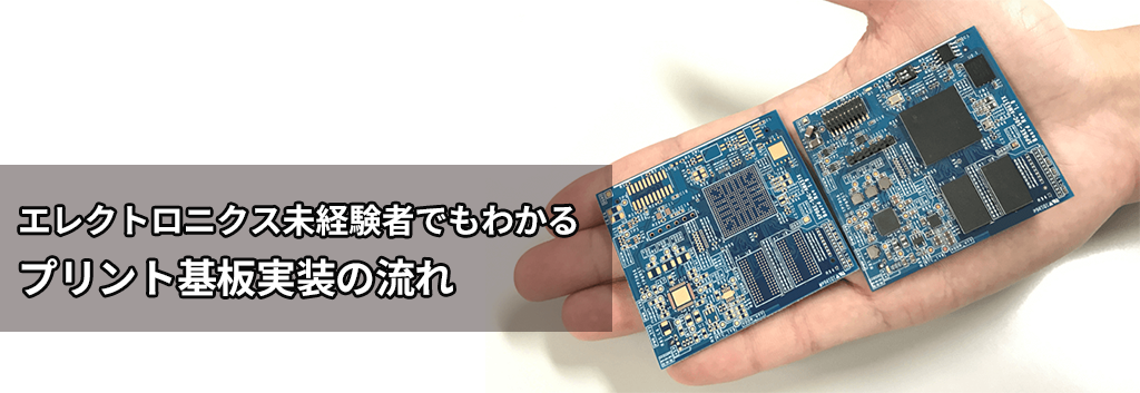
Electronic products contain printed circuit boards to varying degrees, but do you know the manufacturing process?
Have you ever commissioned an electronic circuit assembly factory to do some work for you?
When it comes to printed circuit board assembly, there are a lot of unfamiliar terms, aren't there?
This guide is for beginners who are drawing circuit diagrams, making circuit boards, and assembling components for the first time; for those who had a vague understanding but suddenly found themselves overwhelmed by detailed questions from customers or senior colleagues; and for those looking for ways to reduce assembly costs. We will explain the printed circuit board assembly process with accompanying photos.
If you're interested in Macnica 's manufacturing case studies (mass production utilizing the procurement capabilities of a semiconductor trading company, and the establishment of a global mass production supply system), please refer to the following article.


What is printed circuit board assembly?
Board assembly refers to the process of accurately attaching electronic components such as transistors, capacitors, and IC chips to a printed circuit board (PCB) that has been created based on a blueprint for the electrical circuit, making it function as an electronic circuit.
A printed circuit board only functions as an electronic circuit when a wide variety of components are attached to it. Printed circuit board assembly is a key process that determines the performance and reliability of a product.
The quality and precision of board mounting has a major impact on the lifespan and durability of the entire electronics product, so extremely precise and advanced work is required.
Types and characteristics of printed circuit board mounting
Methods for mounting components on printed circuit boards can be broadly divided into two categories: "SMT (surface mount)" and "DIP (through-hole mounting)." First, let's understand the characteristics of each.
<SMT (Surface Mount Technology)>
This is the current mainstream method of soldering components directly to the surface of a circuit board. Since the leads (feet) are attached directly to the electrodes on the surface of the circuit board without passing them through holes, it allows for miniaturization and high density. It is widely used in products that require lightweight design, such as smartphones and laptops. In mass production, components are efficiently mounted using high-speed automated equipment called a mounter.
<DIP (Dual Inline Package)>
This method involves inserting the leads of components into holes (through holes) attached to the board and soldering them from the back. Although the mounting density is lower than SMT, it has higher mechanical strength and is used in situations where high durability is required, such as for large or heavy components, power circuits, and connectors.
Mounting factories are responsible for this type of board mounting process and mass-produce electronic circuits. From here, we will explain in detail the processes that printed circuit boards go through to mount components and complete electronic circuits.
First of all, what is a printed circuit board assembly factory?
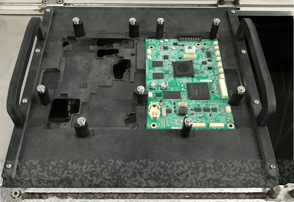
electronic circuit manufacturingboard manufacturingandComponent mountingAfter going through the processes at each factory, the electronic circuit is completed with components mounted on the green board that you see (there are blue, black, and other boards that are not green). I will come.
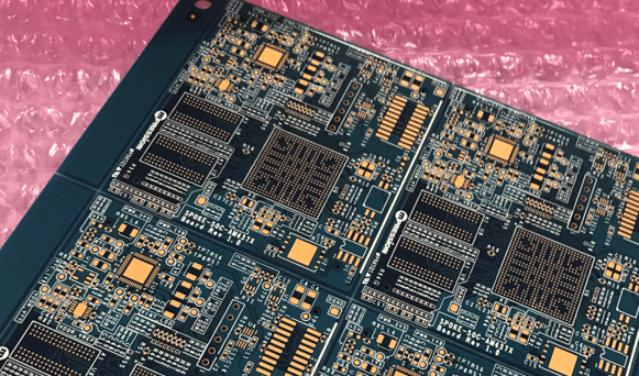
An assembly factory is a factory whose purpose is to mass-produce electronic circuits by assembling components such as ICs and connectors onto printed circuit boards (also called raw boards, bare boards, base materials, or PCBs) that have no components on them, as shown in this photo.
The normal implementation period is about one week to about 10 days.
(Among my fellow designers, this period of time when we are no longer in control is often a time of respite...)
Break down the component mounting process
Now, let's take a look at what goes on inside the assembly factory.
As mentioned above, the process of component mounting is"Mounting surface-mounted components = SMT process"and"Implementing pierced parts = DIP process" can be divided into
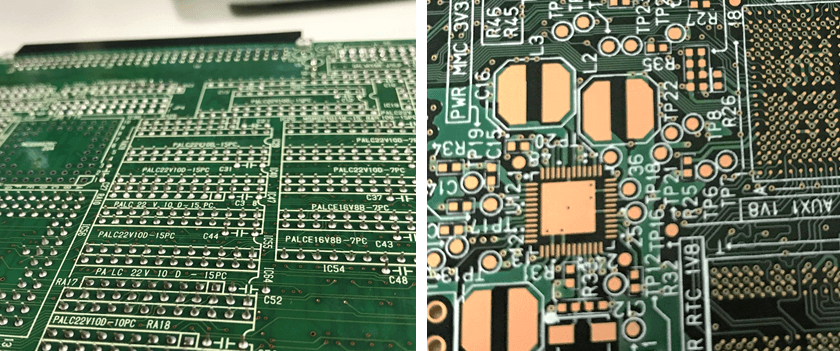
Please remember that when installing a component, if there are holes in the board and the terminals of the component are inserted (photo on the left), it goes through the DIP process, otherwise (photo on the right) it goes through the SMT process. DIP components are hardly seen these days, and your hands don't hurt when holding the board.
The combination of processes is as follows:
・『SMT process only』
・"DIP process only"
・"SMT process + DIP process"
There are patterns like this.
From here, we will explain the procedures and checkpoints for the SMT and DIP processes.
First, the basic process of SMT is to apply cream solder to the printed circuit board, place the components, solder the components, and then inspect the appearance.
Let's take a look at the details.
SMT process (1) Solder material that can be applied Cream solder
The first step in the SMT process for surface mount components is to apply a paste-like solder material called cream solder to the lands of the printed circuit board in preparation for mounting the printed circuit board on an automatic mounting machine.
In electronic work, parts are mounted by melting thread-like solder material with a soldering iron, but cream solder, as its name suggests, is a solder material that is creamy even at room temperature.
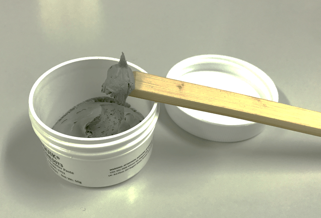
Soldering at room temperaturemelted stateInstead, it is also known as solder paste, which is a mixture of "very fine solder particles" and "flux". Sounds like the name of a special move. Then, a device that applies the cream solder to the printed circuit boardcream solder printing machinecalled.
SMT process (2) Metal mask that determines mounting quality
There is another important point in the process called cream solder printing. This means that you need a metal plate called a metal mask with holes at the same positions as the lands (where you want to solder) on the printed circuit board, as shown in this photo.
When you ask a mounting factory to do the work, it always comes out in the quotation.
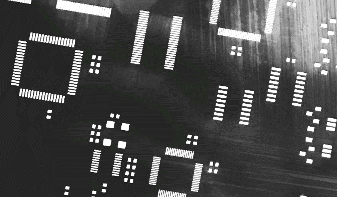
In fact, this metal mask is made quite elaborately, and it is a mass of know-how in mounting quality.
If this is not ideal,
・Nearby pins short circuit
・ void (Bubbles in the mounting part) are formed, resulting in poor contact between the component and the board.
・ Self-alignment does not work due to too much solder solder ball may remain on the substrate as
For semiconductor parts in ultra-small packages, the guidelines include ultra-fine processing instructions in units of tens of microns, such as mask thickness, opening dimensions and shapes, and the addition of slits. The guidelines written in English are Stencil I think it is introduced as
The flow will look something like this.
① Set the printed circuit board in the printing machine
② Cover with a metal mask
(3) Press cream solder from above with a squeegee
④ Remove the metal mask
(5) The board land is coated with cream solder.

(1) Whether it is a prototype or a mass production, it is necessary to create a metal mask when passing through an automatic mounting machine.
(2) Since it is necessary to make a metal mask for each mounting surface of the printed circuit board, when mounting components on both sides of the printed circuit board, two types of metal masks are required, which doubles the cost.
SMT process (3) Mounting (placing) parts
An automatic mounting machine called achip mounter is used to mount hundreds of components on a printed circuit board coated with cream solder.
The chip mounter needs to prepare a program consisting of "image recognition data", "component dimension data", and "board layout data" in advance, and set the components to be mounted on the printed circuit board in a device called a feeder when mounting. Therefore, the more parts there are, the more man-hours for setup.
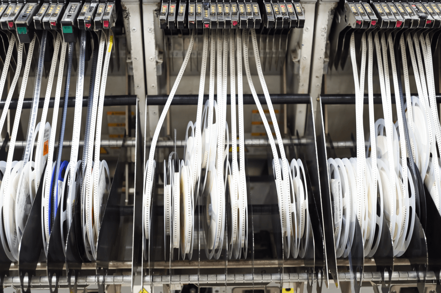
(1) As shown in this photo, the automatic mounting machine is designed so that the rolls packed in a tape shape are pulled into the mounting machine, so even if the required number of tape-cut parts is supplied to the mounting factory, it will not be fed to the feeder. may not be set. In that case, there are cases where additional costs such as "rewinding" and extra man-hours may occur, so in the case of parts supply, I would like to give it to you in a state where you can afford it.
(2) In order to pass through the mounting machine, it takes several hours to set the parts on the feeder with human hands. The number of components to be mounted is important, but reducing the types of components to be mounted also has a large impact on cost.
SMT process ④ Melt the solder in a reflow furnace
The printed circuit board on which the components have been mounted by the chip mounter has not yet been soldered, so it is not yet fixed to the circuit board.
Shaking or swinging the board can cause parts to fly off.
This is where the device that melts the cream solder and securely attaches the components to the circuit board comes in: the reflow oven. Although the word is similar to "flow," which we'll introduce later, it refers to a different process, so be careful.
The temperature inside a reflow oven is controlled, and when a board with components on it passes through, the cream solder melts and completely fixes it to the printed circuit board. Each company has their own know-how for controlling this temperature to improve mounting quality, and they control the temperature inside the oven not only to prevent components from being damaged by heat, but also to maintain mounting quality by maximizing the efficiency of solder melting and flux activation according to a temperature profile.
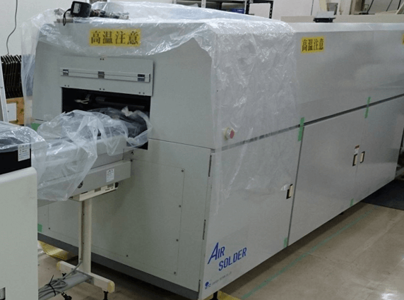
The reflow furnace is like this, functionally it can be called a big oven toaster, the furnace has a length of several meters.
(By the way, the photo is borrowed from the opening ceremony of the reflow furnace.)
I've seen people mounting semiconductors in a toaster oven, and I think it's the same reasoning.
SMT process bonus 1 When reflowing the front and back of the board
In the case of a printed circuit board with SMT components on both sides, the second SMT process is performed with the board turned over after reflow.
Skipping the second SMT step means that two solder prints are required.
But the second solder print is different than the first, do you know why?
The reason for this is that when the first reflow is completed and many parts are already attached to the second solder printing, it is not possible to lay the board horizontally when the first mounted surface faces downward.
At that time, in order to print cream solder on the side where no parts are placed, a jig such as a "printing tray" with a counterbore according to the shape of the mounted parts is required as shown in the photo below. increase. This may not be seen so often by electronic circuit designers.
Therefore, double-sided reflow mounting boards may add costs due to additional equipment.
Depending on the prototype and mounting conditions, such equipment may not be necessary, and there are cases where jigs that can be aligned can be used, so please consult with the mounting factory.
SMT process bonus 2 Which is the front and which is the back?
Slightly digressing from the topic, when reflow-mounting the front and back of the board, we tend to think that we mount the front side first and then the back side, but in reality, we often start from the back side.
Persons in charge of HW design and artwork design have a strong tendency to place large parts, large SoCs, FPGAs, etc. that supplement the main functions of products on the surface unless there are restrictions on the housing situation, right? It makes sense when you think about debugging. (Or, we tend to call the side on which these main parts are placed the "surface", "component side", or "A side")
What do you think would happen if we mounted these heavy parts first and then performed a second reflow? The answer is that when the solder melts again in the reflow oven, the weight of the part causes the part to fall in the reflow oven. For this reason, we have incorporated the idea of reflowing the surface on which heavy parts are mounted in the second reflow process.
It is possible to fix the board and the part by applying a bond so that the part does not fall off even if the solder melts. I'm devising the order of component mounting.
SMT process (5) Visual inspection of the mounted state
After the SMT process, it is necessary to check whether the components are securely mounted.
I think that it can be confirmed to some extent by visual inspection, but in terms of accuracy, speed and quantity, we will use a visual inspection device called AOI (Auto Optical Inspection).
It seems that there are several methods of appearance inspection equipment, but some factories use the latest equipment that supports 3D and inspect the mounting state with tremendous speed and accuracy. In fact, I once asked about the percentage of errors that occurred in the inspection, and it was said that there were no errors, but on the contrary, the accuracy was too good and misjudgment (the state where errors actually occurred) It seems that there are many cases where the inspector confirms that there is no problem), and they said that they still need improvement.
If there is really a problem with the mounting quality, a process such as rework and other measures will be entered by human hands. Also, the inspection process using AOI introduced here is the work to check the state after SMT mounting, but the appearance inspection itself is included in each process.
For example, there are factories that use an optical inspection device called SPI (Solder Paste Inspection) to check the quality of solder printing to make sure that the solder paste is properly pasted even after solder paste printing. If you can check the manufacturing quality so much, you can leave the mass production to us with peace of mind.
DIP process Estimates change greatly depending on how to attach parts
Once the SMT process is complete, the next step is the DIP process for inserting components. Components are inserted into through holes and joined by soldering from the backside.
As explained earlier, the DIP process is a process for mounting components other than the actual surface parts.
Components other than surface-mounted components are called by several names, such as DIP components, pluggable components, lead components, axial components, and radial components, but they can basically be thought of as components that need to be mounted by penetrating the board.
DIP ICs are not seen much these days, but connectors are often DIP products because they need to be strong enough to withstand insertion and removal.
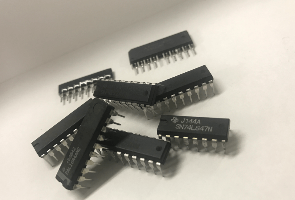
(Nostalgic DIP items that were hard to find)
We will now discuss three implementation methods.
This process is not necessary for boards with only SMT components that do not use DIP products at all.
Based on my experience, there are relatively many manual interventions in the process, so if you consider the production speed and quality, the fewer the parts that need to be pierced, the more stable the production can be expected.
DIP process ① Flow mounting
Flow mounting is a component mounting method that uses a device called a flow tank.
Because the names are similar, people often search for "flow reflow difference" on Google, but the implementation methods involve different work processes.
Reflow ⇒ A method of soldering surface-mounted components
Flow ⇒ Method of soldering pierced parts
The flow tank holds a pool of molten solder, and the DIP components are soldered by jabot-mounting the backside of the board into it. The photo below shows a resin plate called a DIP pallet, DIP carrier, or flow pallet, which is used when performing flow mounting.
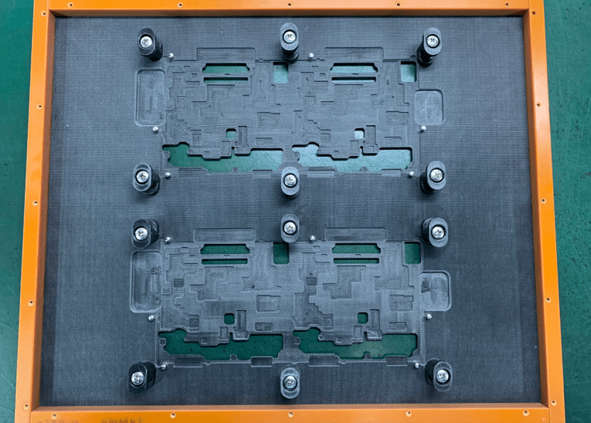
This is an example of a pallet on which 4 boards can be placed. It is profitable to be able to mount 4 cards at once.
Since the pallet is made to cover the parts other than the DIP mounting part like this, there is no danger of solder adhering to other parts. There are also cases to consider and use the following point implementation.
When mass-producing boards with flow mounting, it is necessary to prepare nearly 10 DIP pallets to increase the continuity of production. The initial cost will be in the hundreds of thousands of dollars. Productivity per hour is high, so more electronic circuits can be produced. If you want to use flow mounting, the most important thing is the distance between the surrounding components.
DIP process (2) Mounting by point soldering
It is a mounting method called point soldering, Takurobo, and local soldering.
Flow mounting is also a device used for mounting DIP products, but the difference from flow mounting with a jabot is that a thin metal tube into which solder flows protrudes from the bottom and can be moved by teaching in flow mounting. It enables local implementation that is difficult to deal with.
In point mounting, soldering is done one point at a time by this teaching operation, so it is not suitable for mass mounting manufacturing.
On the back of this black pallet, there is something like a nozzle that jets solder, aiming at the DIP part from the back of the board.
*The reason why the parts are slightly raised is that the temperature profile was analyzed in the reflow process.
As with flow mounting, there are cases where a dedicated pallet is required, but the jig pallet is for the fluxer, and the mounting pallet is only a small number, so point solder mounting is better for the initial investment.
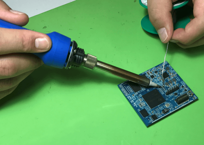
DIP process ③ Mounting method by manual mounting
For mounting that cannot be handled by flow mounting or point mounting, or for manufacturing that does not require machine mounting in the first place, parts may be attached by craftsmen. In many factories, certified professionals are responsible for such manual mounting work. Since it is done by hand, there are no initial costs, and it is simply calculated as mounting man-hours.
Common mistakes and points to note when mounting printed circuit boards
Problems with printed circuit board assembly often occur during the "design stage" rather than the assembly process itself. For example, if the spacing between components is too narrow or the placement of heat-generating components is improper, this can lead to defects and increased costs in later processes, so it is important to review the design data before assembly.
When designing, keep the following points in mind:
- Choose readily available parts (avoid hard-to-source parts)
- Consider the size and shape of the components (whether they are easy to mount)
- Improved heat dissipation pattern (effective in extending the life of heat-generating components)
- Minimize double-sided mounting and DIP components (prevent increases in labor and costs)
By incorporating these ideas from the early stages of design, it is possible to significantly reduce rework in later processes.
Summary
As an extension of our customer development project support, we are sometimes asked to manufacture prototypes and mass-produce products. There was a time when I wondered, "Why does it change so much when it's just soldering?"
With so many options for mounting methods and equipment input, it makes sense that estimates and processes would change depending on the mounting factory. I think it's a little subjective, but I think it's like this.
|
process |
surface mount |
DIP product mounting |
||
|---|---|---|---|---|
| Implementation method | Reflow | flow | point implementation | hand mounting |
| Initial jig equipment | Metal mask (possibly a print tray) |
DIP carrier (Unnecessary if there are no parts on the back) |
No pallets or jigs | unnecessary |
| jig cost | During ~ | high | low | Nothing |
| Productivity | ◎ | 〇 | △ | ☓ |
Even for startups who are manufacturing electronic circuits for the first time for mass production, if they understand the mounting flow and initial equipment, they will not affect the product concept. Don't put the front and back randomly!"
Well, this time, I briefly introduced the mounting process and equipment until the electronic circuit is completed in "The flow of printed circuit board mounting that even people with no electronics experience can understand." How was it?
Depending on the factory, there may be differences from the introduced content, such as "this work or equipment is not available", "the order of work is different", or "additional XX is being done". I think that such places are also packed with the know-how of each factory.
Are you having any problems with production?
As mentioned at the beginning, in addition to semiconductor procurement and technical support, we also provide development planning and manufacturing services centered on the semiconductors we handle.We specialize in small-lot, high-mix production, as well as medium-scale production of several hundred units, and we will meet your needs with the added value that only a semiconductor trading company can offer, such as the ability to select parts that are resistant to discontinued production, so please feel free to contact us.
Manufacturing consulting service
We also provide "manufacturing consulting services" that support not only manufacturing but also the design and planning stages.
- Turning ideas into reality: Proof of concept (PoC) support
- Product development with mass production in mind achieves both performance and productivity.
- We have established a highly responsive and attentive support system and a global mass production supply system.
We have a system in place that allows us to provide one-stop consultations from the early stages of development through prototyping and mass production, so please feel free to contact us if you have any concerns or issues regarding board mounting. For more information on our manufacturing consulting services, please click the button below.

