- Semiconductor BusinessHOME
- Products and Services of Macnica,Inc.
-
technical information

-
Events and Seminars
- Handling Manufacturer
- Support
- Inquiry
- Click here to purchase products
- Semiconductor business e-mail magazine registration
![]()
![]() Narrow down by specifying conditions
Narrow down by specifying conditions
現在2159件がヒットしています。check
Stripline = middle layer
Continuing from the last time, I will consider the strip line.
The number in the figure is the serial number from the previous time.
Many approximations have been proposed for striplines.
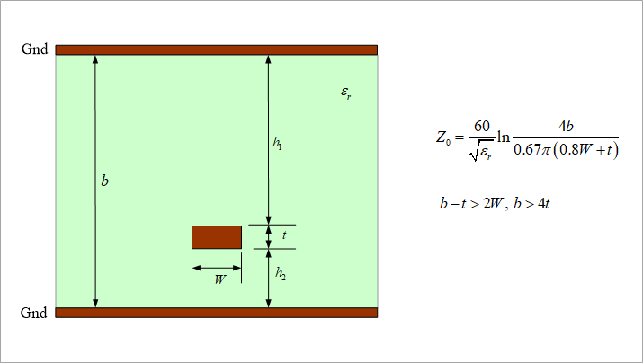
The formula shown in Figure 9 is often used.
In addition to the dielectric constant εr, the parameters are only the distance b between grounds, the pattern width W, and the pattern thickness t.
The distance between the pattern and the ground, h1 and h2 are not mentioned.
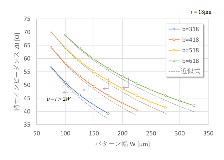
Figure 10 plots the values of the approximation formula when the distance b between the grounds is changed and the pattern is in the center of both grounds, i.e. h1=h2=(b-18)/2. .
One of the conditions, bt > 2W, is within a small error.
Another condition, b>4t, is fully satisfied because t=18um.
However, in reality, the pattern is not in the center of both grounds, so I don't think it makes much sense from a practical point of view.
As an actual example, for example, in a 6-layer board, when the h of the surface layer is 300um and the board thickness is 1.6mm, the b of the intermediate layer is b=1,600-2(85+h), so b=830um. becomes.
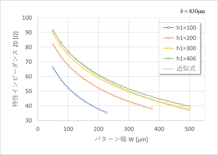
Fig. 11 compares the approximation formula and the analytical value when h1 in Fig. 9 is changed under these conditions.
If h1=300um or h1=406 (centered), the approximations are pretty good.
Even for strip lines, the approximation formula is based on the assumption that h1 is large, and the current h1 = 100um or 200um deviates from the analytical value.
give up approximation
It seems that many of the approximation formulas for microstrip lines and strip lines were announced in the 1960s. At that time, analytical methods and the processing power of the computers needed to implement them were poor, so approximation formulas were of great significance. After that, the substrate manufacturing process became finer, and the conditions of the approximation formula at that time were far from being met.
Now that the analysis methods and the processing power of computers as engines have improved dramatically, I believe that proper analysis should be done instead of approximation formulas.
The tool is in the situation described earlier.
Therefore, using the tools I own, I created an Excel sheet for obtaining cross-sectional dimensions from the required specifications.
The condition is
Characteristic impedance is 50Ω
Differential impedance is 85Ω
is.
For practical purposes, I think this is sufficient.
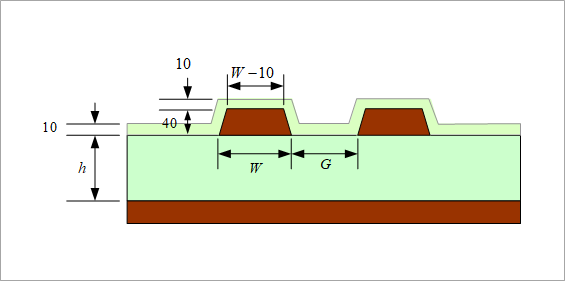
Figure 12 shows the cross section of the microstrip line to be analyzed.
Conductor thickness is 40 μm, narrow trapezoidal shape
Solder resist thickness 10 μm (shape of (b) in Fig. 8)
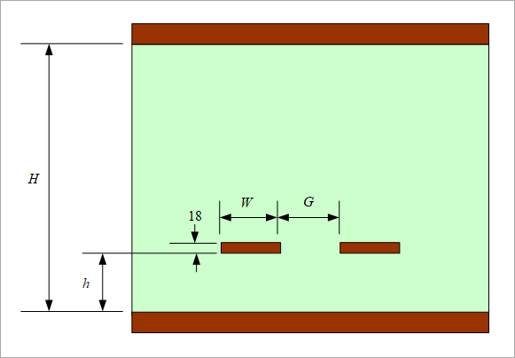
Figure 13 also shows a cross section of a strip line.
Conductor thickness is 18 μm, rectangular
Depending on the lamination method, the intermediate layer will have a trapezoidal shape facing upwards or downwards.
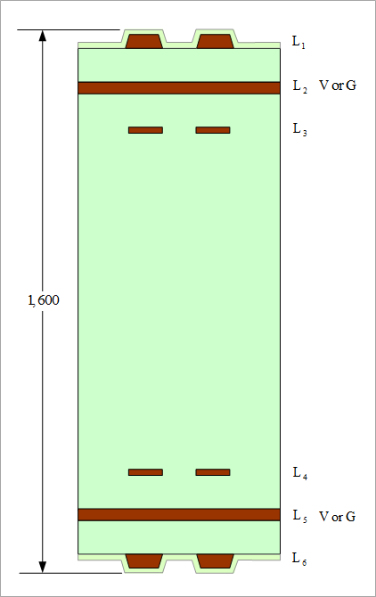
Figure 14 is an overall view of a 6-layer board.
Determine H in Fig. 13 by taking the total plate thickness as the standard 1,600 μm (1.6 mm) and subtracting the thickness of the surface layer.
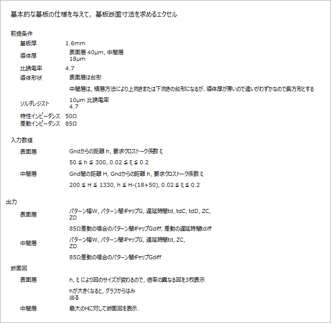
Figure 15 is an explanation of the Excel sheet that determines the cross-sectional dimensions of the board.
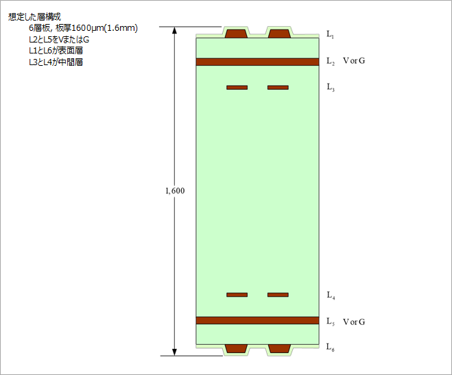
Figure 16 shows the assumed layer structure of the Excel sheet.
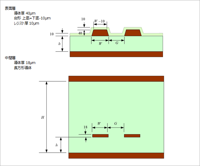
Figure 17 shows an assumed cross-section of the surface layer and intermediate layer.
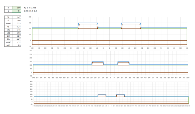
Figure 18 is an example of surface layer analysis. Some dimensions extend beyond the screen, so they are displayed in three scales.
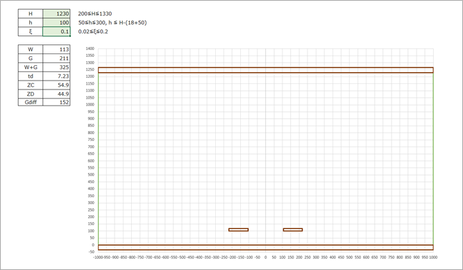
Figure 19 shows an analysis example of the middle layer.
This tool is still in beta version and not open to the public.
If you want to use this tool, please read the message from the author in the last column.
What is Yuzo Usui's Specialist Column?
It is a series of columns that start from the basics, include themes that you can't hear anymore, themes for beginners, and also a slightly advanced level, all will be described in as easy-to-understand terms as possible.
Maybe there are other themes that interest you!