
![]()
![]() Narrow down by specifying conditions
Narrow down by specifying conditions
現在1888件がヒットしています。check

We will explain the keywords related to the electrical characteristics of crystal oscillators. We will also explain specific numerical values, calculation methods, and information on the manufacturing process.
1. Frequency deviation (normal temperature deviation)
It is the degree of frequency deviation at 25°C. It is determined by the accuracy of work in the frequency adjustment process. For general applications, it is about ±30ppm or ±50ppm, but for wireless communication, a strict deviation of ±10ppm may be required.
Considering manufacturing variations, ±8ppm or ±7ppm is the strictest level at the mass production level. The stricter the standard, the lower the yield and the higher the unit price.
| Freq. Range Frequency range |
Freq. Tolerance frequency deviation |
Freq. Stability Frequency stability |
Operation Temp Range Operating temperature range |
Drive Level drive level |
| 16.000MHz~ 69.999MHz |
±10ppm, ±50ppm (at 25°C) |
±10ppm, ±50ppm (Ref. to 25℃) |
-10°C to +60°C -40°C to +85°C *1 |
100μW max. |
| 70.000MHz~ 200.000MHz |
±30ppm, ±50ppm (at 25°C) |
±30ppm, ±50ppm (Ref. to 25℃) |
-10°C to +60°C -40°C to +85°C |
2.0μW typ. (100μW max.) |
*1 ±15ppm product or more
(Reference) Kyushu Dentsu: MAS series data sheet
2. Frequency temperature characteristics
It is the degree of deviation of the frequency with respect to temperature changes when the value at 25°C is used as the standard.
For AT-Cut crystals, draw a cubic curve.
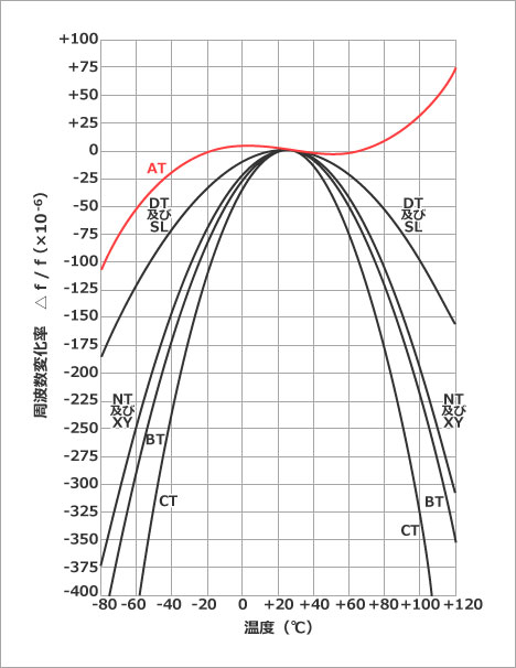
The frequency temperature characteristics are determined by the accuracy of the cutting angle of the crystal blank.
Normally, blanks within ±3' or ±1' are used for the specified cutting angle, but when severe temperature characteristics are required, blanks within ±15" or ±7.5" are used. will be used.
As an example of the limit of temperature characteristics at the mass production level, it is generally said as follows.
(-5 to 50°C) ±3ppm
(-10 to 60°C) ±5ppm
(-20 to 70°C) ±7.5ppm
(-30 to 80°C) ±15ppm
(-40 to 90°C) ±20ppm
The stricter the standard for frequency temperature characteristics, the worse the yield, and the higher the unit price.
3. Equivalent series resistance
ESR = Equivalent Series Resistance, also known as Rs or R1.
Crystal oscillators act as resistors that make it difficult for current to flow through them. This is called equivalent series resistance and is expressed in Ω. (Resistance value measured by crystal alone without load)
The smaller the ESR value, the easier it is to oscillate. However, if an ESR that is stricter than the standard is required as a standard, the yield will deteriorate and the unit price will increase.
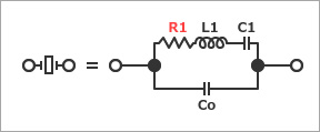
R1: Equivalent Series Resistance
L1: Equivalent Series Inductance (Motional Inductance)
C1: Equivalent Series Capacitance (Motional Capacitance)
Co: Shunt Capacitance
In order for a crystal unit to oscillate, it is necessary to have the power to cancel the resistance component of the crystal in the IC of the oscillation circuit and start the oscillation. This oscillation starting power is called the negative resistance (-R), and the unit is Ω. represented by .
The larger the negative resistance, the easier it is to oscillate (also expressed as oscillation margin).
Click here for negative resistance and oscillation margin.
[Basic lecture on crystal units] Oscillation conditions and circuit matching (circuit analysis)
4. Load capacity (CL)
Load capacitance is the capacitance of the entire oscillation circuit, excluding the crystal unit. (circuit load capacity)
In order for the oscillator to oscillate properly, the crystal oscillator must be manufactured to match the load capacitance of the circuit. (Crystal oscillator load capacity = circuit load capacity)
4-1. Load capacity value
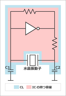
The value of the load capacitance when using a crystal unit with a fundamental wave can be calculated using the following formula.
*C1 and C2 are the values of the two capacitors in the oscillation circuit
Unless you actually measure it, you can't know exactly what the capacitance of the IC is, but it's usually 4 to 5 pF. (Strictly speaking, it is the capacitance between the 2 pins of the IC + the board pattern capacitance)
For example, in the oscillation circuit, if C1 and C2 are 8pF,
Calculating this gives CL=8 or 9pF.
From this calculation, it can be seen that this circuit will oscillate almost exactly if a resonator with a load capacitance of 8 or 9 pF is installed. Since the above values are obtained only by calculation, it is necessary to analyze the actual circuit in order to obtain the actual optimum value (this is called circuit analysis or circuit matching).
4-2 Relationship between load capacitance and frequency change
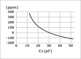
The relationship between load capacitance and frequency change shows a hyperbola like the one on the right. The figure on the right is an example of 10MHz, where the X-axis shows the load capacitance of the circuit and the Y-axis shows the frequency deviation.
It is 0ppm at 30pF, but when the capacitance changes, the frequency also changes plus or minus.
This rate of change draws different curves depending on package size, frequency, electrode size and other factors.
By changing the load capacitance (specifically, by changing the value of C in the circuit), the oscillation frequency can be changed. (The smaller the load capacitance value, the larger the frequency change rate.)
If you do not install a crystal with an appropriate load capacitance value, frequency deviation and other problems will occur.
5. Excitation level (drive level)
It is the power to oscillate the crystal. If the drive level is set too high, spurious emissions are likely to occur and oscillation may become unstable.
Also, if the drive level is too high, it may cause abnormal jump fluctuations in frequency and series resistance in temperature characteristics, so be careful. Less than 3µW, or too low, can also cause problems.
As a rough guideline, about 100 µW is desirable, but it varies slightly depending on the package size, frequency, specifications, and other factors. In order to find the optimum value, it is still best to analyze the actual circuit.
Click here for recommended articles/materials
[Crystal Oscillator Basic Lecture] Explanation of terms related to the electrical characteristics of crystal oscillators
[Basic lecture on crystal units] Oscillation conditions and circuit matching (circuit analysis)
[Crystal Oscillator Basic Course] Concrete Examples of Circuit Matching (Circuit Analysis)