Introduction
hello. It's phi.
Last time, I finally got my hands on it.
This time, I would like to introduce what I stumbled on and what I learned about "layout design".
Before that, what is “layout design” in the first place?
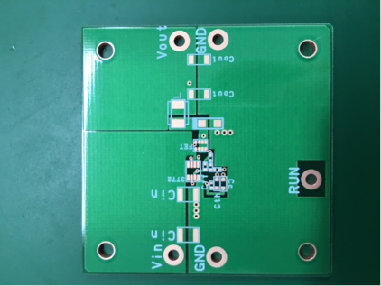
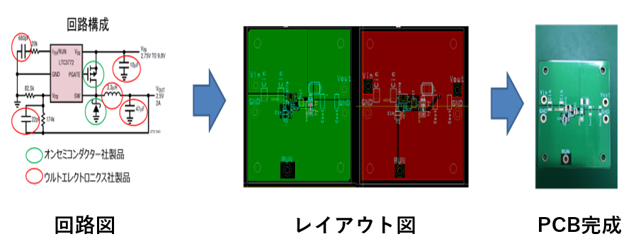
It is to lay out the circuit on a printed circuit board (PCB board) as shown in Fig. 1 based on the circuit diagram you made.
Figure 2 shows an overview of the layout design.
At first glance, it seems easy, but when I actually tried it, there were many things I didn't understand, and I had a lot of trouble. .
i don't know how to layout
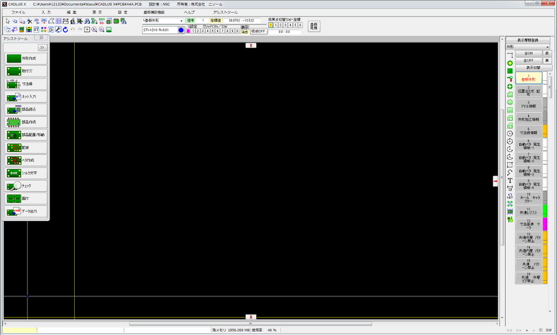
I immediately decided to draw a circuit using PCB layout design software (Fig. 3).
But here is the first stumbling block.
“How should the circuit be laid out?”
I had no clue, so I went to ask my seniors.
Fai: I'm sorry, but I have no idea how to draw the circuit...
Senior: “Where a large current flows, the wiring should be thick and straight! The bend should be 45 degrees!”
Fai: "Why???"
Senpai: “Try to feel like an electron!”
Fai "???"
After that, I spent days thinking about the feelings of electrons.
Keep Thinking After 3 days, I finally found out why!
When a large current flows (when the number of electrons is very large), if the wiring is thin or twisted, the electrons will collide with each other and cannot move forward.
Also, if the bend is too sharp, the electrons will use up extra energy when they bend (release it as heat), which will reduce energy efficiency. It's the same as when a car has a hard time speeding up on a sharp curve (you need to step on the brakes).
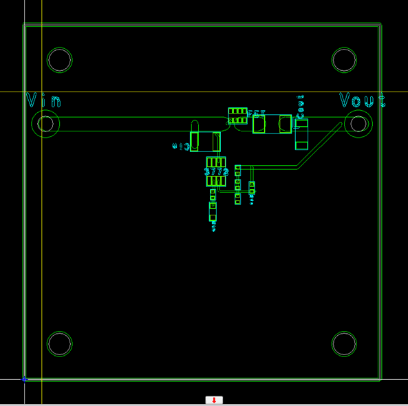
Now that I understood the feelings of electronics, I created a layout diagram based on the advice of my seniors (Fig. 4).
But here comes the next problem. . .
wiring too thin
If you have a senior look at the layout diagram in Figure 4,
Senior: “This layout diagram is very unstable, so I don’t think it will work well.”
Me"????"
Senior: “You can compare it with the layout diagram on the evaluation board.”
After that, I quickly compared my circuit with the layout diagram of the evaluation board (Fig. 5).
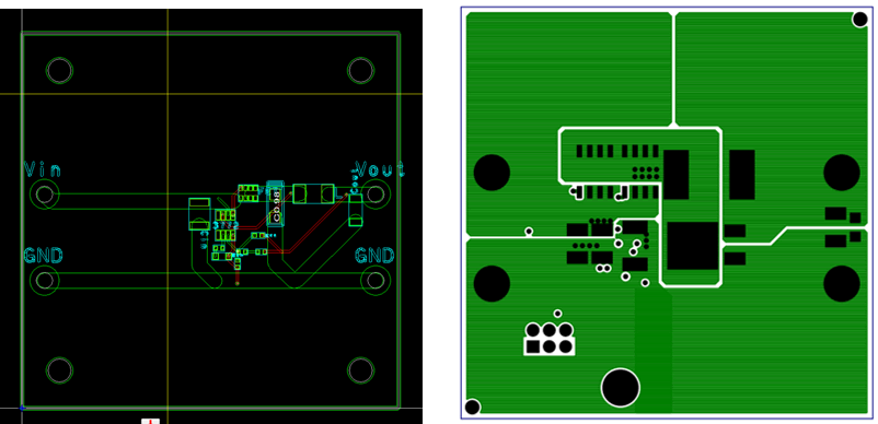
As shown in Figure 5, my circuit has very thin wiring (green part), while the evaluation board has wiring spread over the entire board (thick wiring is drawn), and the entire board is green. has become
At first, I thought that if the wiring was too thick, the electrons would travel in a roundabout way.
So I tried to wire it as straight as possible.
However, upon closer examination, it was found that thin wires are more susceptible to noise.
Taking the precautions mentioned above into account, I redraw the circuit again and finally completed it (Fig. 6)!
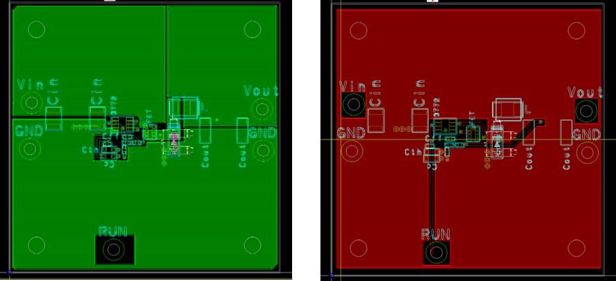
This should be fine...! !
Summary
・When drawing a circuit, make the wiring thick and straight where a large current flows.
⇒Because electrons flow stably
・Where the wiring bends, set the angle to 45 degrees.
⇒To avoid wasting energy when electrons bend (to suppress heat release)
・Because the PCB board has thin conductors, the thickness of the wiring should be as thick as possible.
⇒ If it is too thin, it may break in the middle.
through layout design “Circuit design should feel electronic” I learned the importance of
Next time, it's finally time to implement! looking forward to! !
<On a side note...>
Actually, I had a lot of trouble when using "PCB layout design software".
I just stared at the instruction manual and managed to understand how to operate it.
It is important to try everything first.

