- Semiconductor BusinessHOME
- Products and Services of Macnica,Inc.
-
technical information

-
Events and Seminars
- Handling Manufacturer
- Support
- Inquiry
- Click here to purchase products
- Semiconductor business e-mail magazine registration
![]()
![]() Narrow down by specifying conditions
Narrow down by specifying conditions
現在2189件がヒットしています。check

Introduction
Hello. This is Phi.
From this time on, I would like to introduce what I learned and what I stumbled upon during the "production training" that is part of the training for new employees.
Manufacturing training is something new FAEs who have joined Macnica must do, and the purpose is to deepen their understanding of semiconductors through manufacturing.
Make your own DCDC converter!
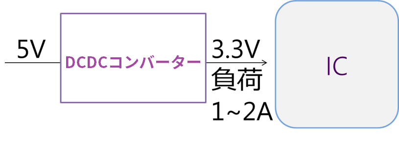
I made a DCDC converter to deepen my knowledge of analog products. Specifically, it is a step-down converter that converts 5V to 3.3V as shown in Figure 1.
DCDC converters are always included in electronic devices such as smartphones and personal computers that everyone has.
Learn more about DCDC converters here.
This time, I will introduce the general flow of making a DCDC converter.
How a DCDC converter is made
The process of creating a DCDC converter is as follows.
(1) Parts selection
②Hand assembly (prototype)
③ Pattern design
④ Implementation
⑤ Evaluation (test)
I will briefly explain each of them.
①Parts selection
First decide which parts to use.
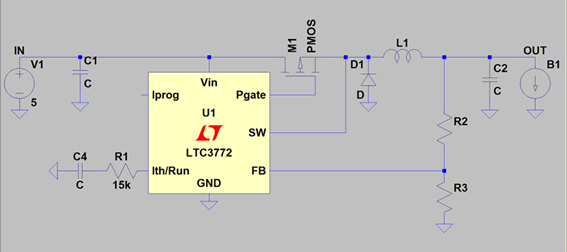
Basically, select from important parts, and if it is a DCDC converter, select from the power supply IC.
I decided to use LTC3772 as power supply IC.
After deciding on a power supply IC, I selected peripheral components (MOSFETs, inductors, diodes, etc.).
②Hand assembly (prototype)
Once the parts have been decided, the next step is hand assembly (prototyping). The main reasons for doing this are:
1. To check if the parts work together
2. To reduce the cost and time of pattern design
I assembled it by hand using a universal board (Fig. 3).
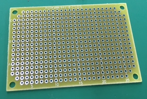
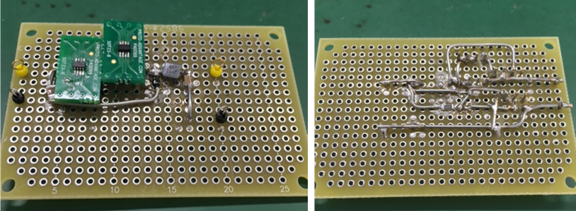
Figure 4 shows the board that was actually manufactured.
③ Pattern design
Once it is determined that the parts can be used after hand assembly, pattern design is carried out.
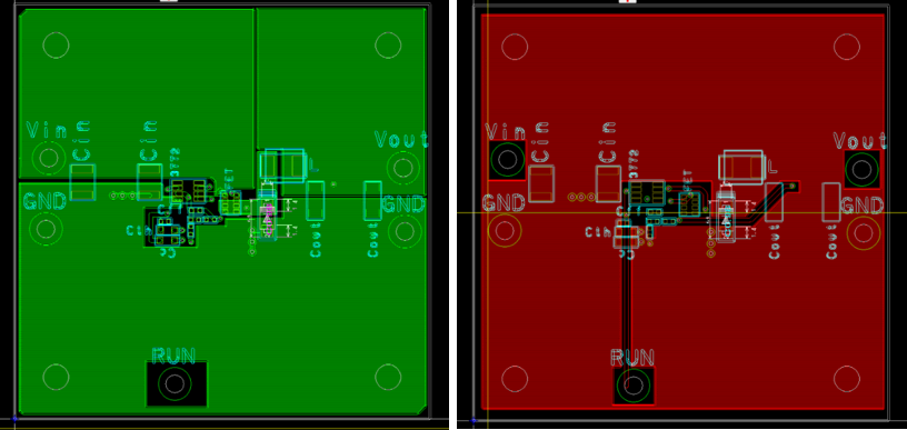
Pattern design is to create a circuit in the PCB board as shown in Figure 5.
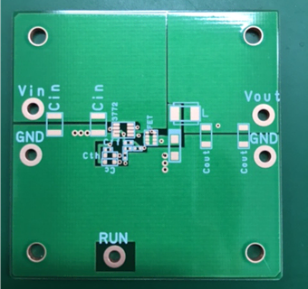
I drew a circuit as shown in Fig. 6 and placed an order.
④ Implementation
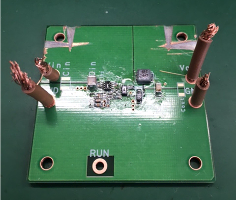
For mounting, the parts are placed on the land of the PCB board and soldered.
During mass production, all mounting is done by machine, but I soldered the parts manually (Fig. 7).
I ran into a lot of problems with the implementation and had a lot of trouble. I would like to introduce this in a future blog.
⑤ Evaluation (test)
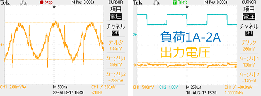
We evaluated (tested) whether the completed product worked correctly.
Evaluation items vary depending on the product, but in the case of power supplies, we often look at ripple voltage and load response.
Figure 8 shows the measurement results when I actually evaluated it.
Set makers must evaluate their products in this way and confirm that they work as expected.
This is where problems often arise and designers struggle.
I also faced a lot of difficulties during the evaluation stage (the production practice was the biggest climax).
Summary
This time, I was able to learn again what the customer (set maker) is doing through the production training.
From the next time, I would like to take up more and more problems that actually occurred in the production practice. looking forward to! !