- Semiconductor BusinessHOME
- Products and Services of Macnica,Inc.
-
technical information

-
Events and Seminars
- Handling Manufacturer
- Support
- Inquiry
- Click here to purchase products
- Semiconductor business e-mail magazine registration
![]()
![]() Narrow down by specifying conditions
Narrow down by specifying conditions
現在2186件がヒットしています。check

In order to obtain stable operation within the specifications of a DC/DC converter, one of the important factors is the loop characteristics, i.e. the phase margin and gain margin of the internal error amplifier.
In this article, we will discuss mutual interference (large change in phase margin characteristics) when using the 2-channel DC/DC converter LT8650S and using channel 1 (CH1) with an internal compensation circuit and channel 2 (CH2) with an external compensation circuit. We will introduce the results of verifying that this does not occur.
Power specifications and features of the device used
Power supply specifications
The required specifications and devices used for this power supply circuit are as follows.
・Input voltage (Vin)|12(V)
・Output voltage/current | Vout1: 5(V)/0.2(A), Vout2: 3.3(V)/0.25(A)
・Switching frequency | 2 (MHz)
・Device used | Step-down DC/DC converter with built-in 2-channel synchronous rectification power element (LT8650S)
Features of the device used
The device used, LT8650S, has a built-in compensation circuit, so it can be used without placing an external phase adjustment capacitor or resistor.
Devices with built-in compensation typically do not provide pins for external compensation. However, the LT8650S is unique in that it has a built-in compensation circuit and an externally adjustable VC pin.
With this VC pin, it is possible to connect an external capacitor and resistor to improve phase margin and load response.
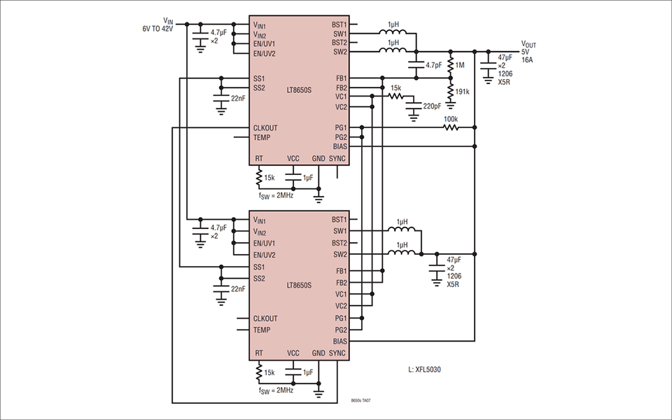
Additionally, since the output current can be balanced using the VC pin, it is also possible to prepare two LT8650S and connect them in parallel as shown in Figure 1 to support 16A output.
Verification against capacitance change of output capacitor
When using internal compensation circuit for both channels
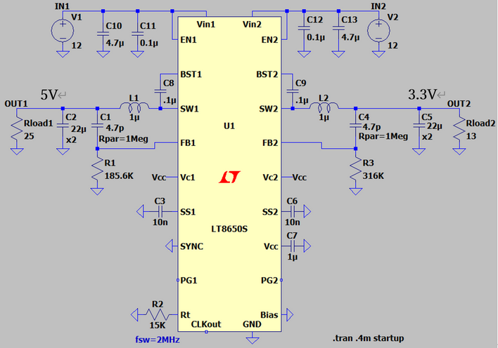
Figure 2 is a circuit diagram when using internal compensation circuits for both channels with Vout1=5(V), Vout2=3.3(V) settings.
*Although all the circuit diagrams in this article are written in LTspice, all phase margins are the results of measurements using actual equipment.
The output capacitor has been changed from the recommended 47uFx2 to 22uFx2.
We actually measured how much phase margin there would be at this time.
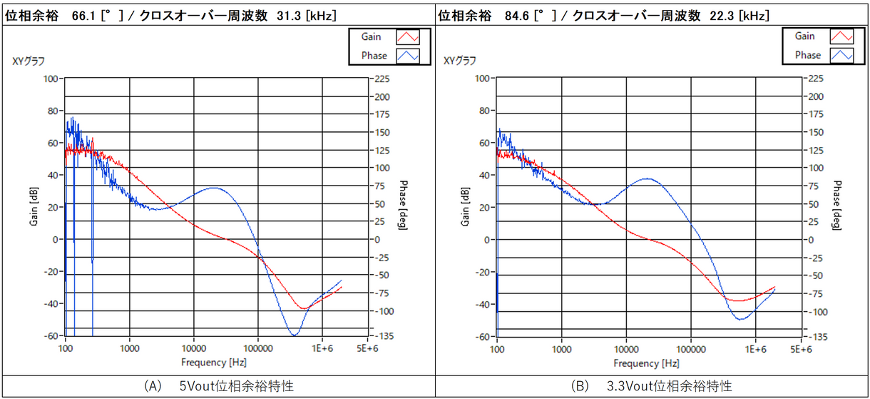
When measuring 5Vout of CH1, 3.3Vout was turned off, and when measuring 3.3Vout of CH2, 5Vout was turned off, taking into account the possibility of internal interference occurring.
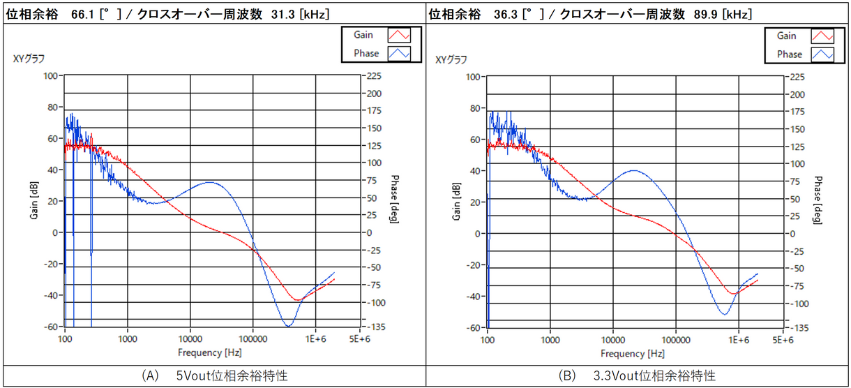
Phase margin when using internal compensation circuit for both channels
5Vout has a sufficient phase margin of 66.1 degrees. 3.3Vout is 36.3 degrees, which is well below the 45 degrees that is said to be the general stable area, so adjustment is required to ensure sufficient phase margin.
The main means is to change the constants of the feedforward capacitor, inductor constant, and output capacitor, but since changing the inductor and output capacitor in particular greatly affects other power supply characteristics, it is possible to switch to an external compensation circuit and make adjustments. Let's try to secure the phase margin within the range.
3. Consideration of external compensation circuit for 3Vout
Checking the phase margin by changing the external compensation circuit
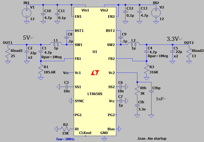
Figure 4 is a circuit diagram when Vout2 is changed to an external compensation circuit with Vout1=5(V), Vout2=3.3(V) settings.
I connected Rth=3KΩ, Cth=3.3nF, Cthp=1nF to the VC2 pin as an external compensation circuit.
We actually measured how much phase margin there would be at this time.
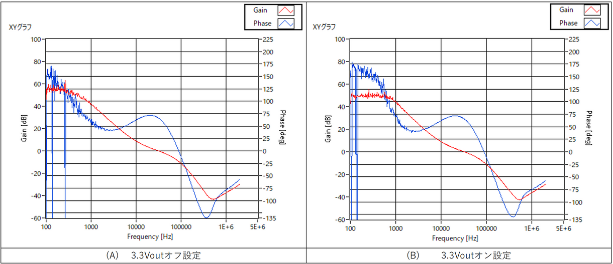
When measuring 5Vout of CH1, 3.3Vout was turned off, and when measuring 3.3Vout of CH2, 5Vout was turned off, taking into account the possibility of internal interference occurring.
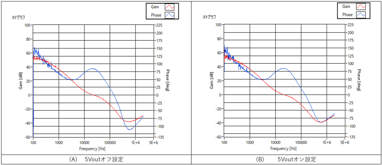
5Vout is the same as the previous circuit, so there is no change.
3.3Vout was adjusted using an external RC compensation circuit, and a sufficient phase margin of 84.6 degrees was secured.
The crossover frequency is low at 22.3KHz, and further adjustment is required when high-speed load response is required.
However, since it was outside the main purpose of this time, we did not make any adjustments.
Check the phase margin characteristics with both channels on
Using the circuit in Figure 4 as is, this time we measured the phase margin with both channels on. The measurement results were as follows. Figure 6 shows the phase margin characteristics for 5Vout, and Figure 7 shows the phase margin characteristics for 3.3Vout, and there are no major changes in the phase margin characteristics due to turning on and off of adjacent channels.
This suggests that when using internal/external compensation for each channel of the LT8650S, the effect on phase margin characteristics is extremely small, and it is basically possible to use a mixture of internal/external compensation.
supplement
I would like to add that this description is for the LT8650S and may not apply to all 2-channel DC/DC converter devices.
The LT8650S has a block for each CH1 and CH2, and the error amplifier and surrounding architecture are also separate, so we would also like to note that they are not shared in the same block. See the LT8650S data sheet for more information.
Click here for recommended seminars/workshops
Click here for recommended articles/materials
LTspice List of articles: Let's use LTspice series
FAQ about power ICs: FAQ list
List of technical articles: technical articles
Manufacturer introduction page: Analog Devices, Inc.
Click here to purchase products
Click here for manufacturer site/other related links
Inquiry
If you have any questions regarding this product, please contact us using the form below.
Analog Devices Manufacturer Information Top
If you want to return to Analog Devices Manufacturer Information Top, please click the button below.