- Semiconductor BusinessHOME
- Products and Services of Macnica,Inc.
-
technical information

-
Events and Seminars
- Handling Manufacturer
- Support
- Inquiry
- Click here to purchase products
- Semiconductor business e-mail magazine registration
![]()
![]() Narrow down by specifying conditions
Narrow down by specifying conditions
現在2189件がヒットしています。check

In the DC/DC converter circuit design, it may be necessary to improve the load response depending on the specifications of the microcomputer or FPGA. In such cases, I think the easiest way to improve the load response characteristics is to increase the capacity of the output capacitor.
However, when you actually move to board design, you may find it necessary to reduce the number of output capacitors to increase the mounting area. At times like this, we sometimes receive questions from customers, such as, "Is there no problem if we reduce the number of capacitors?"
This time, we will verify whether the problem occurs when the number of output capacitors is reduced.
Evaluation environment
This time, we used the LT8643S evaluation board (DC2658A), which is a 42V withstand voltage synchronous rectifier MOSFET built-in step-down DCDC from Analog Devices.
Evaluation board settings
The modification of the original evaluation board is to change the phase compensation circuit to the optimum value.
Before change: R4=8.45kΩ C5=0.33nF
After change: R4=6.3kΩ C5=1.36nF
Evaluation conditions: Input voltage 12V, output voltage 5V, load current 3A, switching frequency 2MHz setting
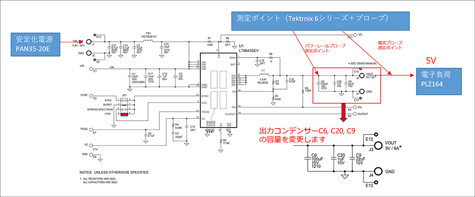
Measurement environment
- Stabilized power supply KIKUSUI PAN35-20E is used. Connect between VIN and GND on the evaluation board
・Uses electronic load KIKUSUI PLZ164WS. Connect between VOUT and GND
・Oscilloscope Tektronix 6 series is used. Ripple observed across output capacitor C6
- With Power Rail Probe TPR1000.
- Accessory 1.3m, SMA(Ma) - MMCX (Ma) , 50Ω cable
- Accessory MMCX connector (Wurth Elektoronik 66012002111503)
Verification against capacitance change of output capacitor
When the capacity of the output capacitor is reduced
In the initial state of the evaluation board, the phase margin is not optimal, so we changed the compensation circuit.
R4 and C5 in the circuit diagram of Figure 1 were changed as follows, and the phase margin was improved from 56° to 81.5°.
Before change: R4=8.45kΩ C5=0.33nF ⇒ After change: R4=6.3kΩ C5=1.36nF
After optimizing the phase margin, change the output capacitor (C6) from 123uF ⇒ 45uF ⇒ 23uF and confirm the output voltage. The result is the ripple waveform in Fig. 2.
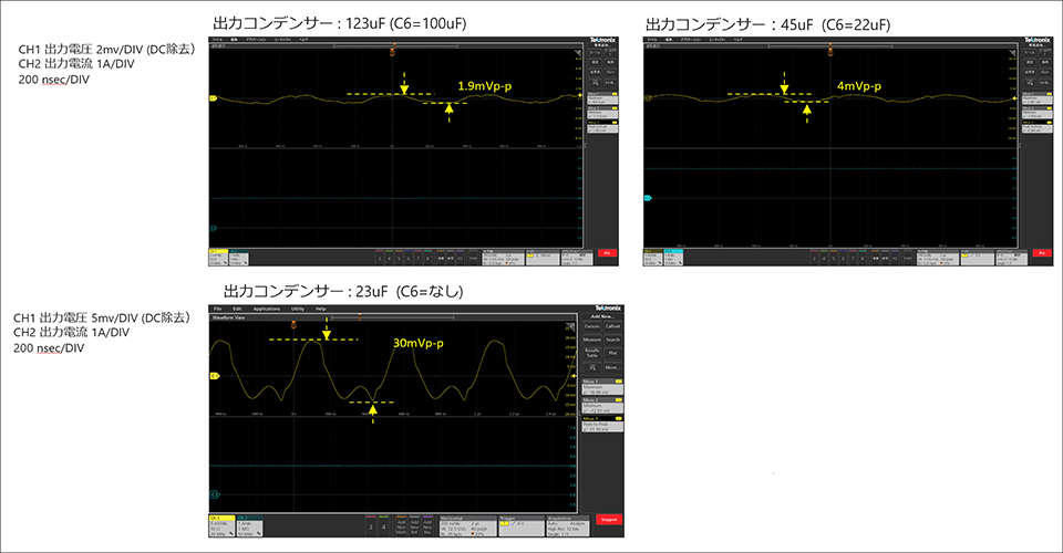
Result of changing the capacity of the output capacitor
When I changed the output capacitor from the default setting of 123uF to 45uF, the ripple voltage increased from 1.9mV to 4mV. If the ripple voltage is acceptable, it is possible to reduce the output capacitor capacity to 45uF.
However, when the capacitor capacity was reduced to 23uF, the output ripple increased to 30mV and the output voltage became unstable (slightly oscillating).
From this result, it can be seen that the output voltage becomes unstable if the output capacitor is made small easily.
Next, let's check if the phase compensation circuit is in the optimum state when the output capacitor is 45uF.
Compensation Network Optimization for Output Capacitor
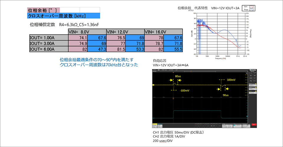
Phase margin and load response when output capacitor is 163uF
Figure 3 shows the measurement results of the phase margin and load response characteristics when the output capacitor is 163uF.
The phase margin was 74.1 to 82°, and the voltage fluctuation was ±100mV (crossover frequency 71.8KHz) when checking the load response characteristics.
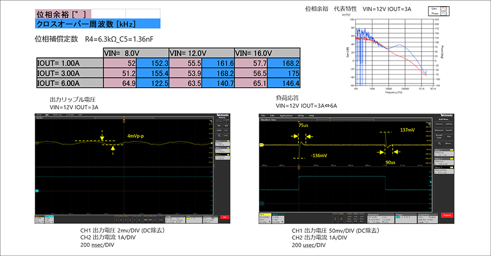
Phase margin and load response when output capacitor is 45uF
Figure 4 shows the measurement results of the phase margin and load response characteristics when the output capacitor is 45uF.
The phase margin was 51.2° to 65.1°, and when checking the load response characteristics, the voltage fluctuation was about ±137mV (crossover frequency 168.2KHz).
The phase margin has decreased by about 20°. From this result, you can understand that the phase margin changes by changing the capacity of the output capacitor.
Optimization of phase compensation circuit
Figure 5 shows the result of optimizing the phase compensation circuit when the output capacitor is 45uF.
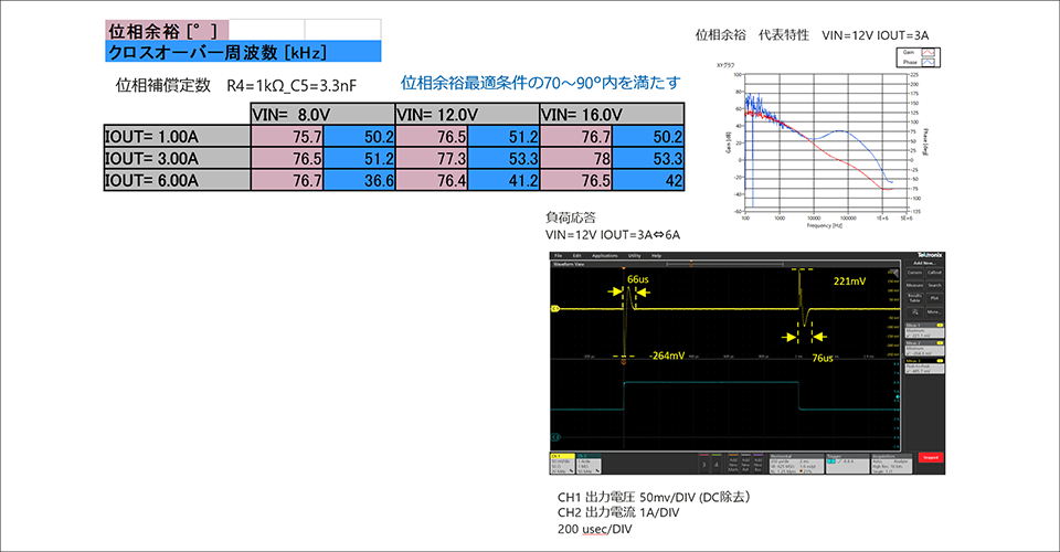
The phase margin was improved from 53.9° to 77.3° by changing R4 and C5 in the circuit diagram of Fig. 1 as follows.
Before change: R4=6.3kΩ C5=1.36nF ⇒ After change: R4=1.0kΩ C5=3.3nF
However, the crossover frequency increased from 168.2KHz to 53.3KHz, the load response characteristics became slower, and the voltage fluctuation increased to +221mV/-264mV.
Summary
Changing the output capacitor capacity may change the phase margin and cause the output voltage to become unstable, so reducing the output capacitor should be avoided.
When changing the output capacitor, it is recommended to check the phase compensation circuit for optimum.
If the capacitance is reduced by reducing the number of output capacitors due to restrictions on the mounting area of the board, changing the compensation circuit constants to obtain a phase margin may lower the crossover frequency and affect the load response characteristics. There is a need to be careful.
Click here for recommended seminars/workshops
Click here for recommended articles/materials
LTspice List of articles: Let's use LTspice series
FAQ about power ICs: FAQ list
List of technical articles: technical articles
Manufacturer introduction page: Analog Devices, Inc.
Click here to purchase products
Click here for manufacturer site/other related links
Inquiry
If you have any questions regarding this product, please contact us using the form below.
Analog Devices Manufacturer Information Top
If you want to return to Analog Devices Manufacturer Information Top, please click the button below.