- Semiconductor BusinessHOME
- Products and Services of Macnica,Inc.
-
technical information

-
Events and Seminars
- Handling Manufacturer
- Support
- Inquiry
- Click here to purchase products
- Semiconductor business e-mail magazine registration
![]()
![]() Narrow down by specifying conditions
Narrow down by specifying conditions
現在2186件がヒットしています。check

When using an FPGA with a large circuit scale, the amount of current that the FPGA requires from the power supply increases.
As a result, the amount of current required in the power circuit also increases.
Parallel connection of switching regulators
As the power demanded by the FPGA increases, there are cases where the switching regulator circuit or module with a single current value of the original 12V power supply does not have enough capacity.
In such a case, it will be necessary to change the switching regulator used and consider a circuit that can output a large capacity.
Considering a new power supply circuit is one solution, but another solution is to cover the current capacity by running a power supply circuit that has a proven track record in parallel.
The point to be noted here is to confirm whether the power supply circuit can be operated in parallel.
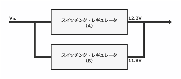
When the power supply circuits are operated in parallel by simply connecting the outputs as shown in Fig. 1, if the output of switching regulator (A) is 12.2V and the output of (b) is 11.8V as shown in Fig. 1, If you connect the output and pull the load, the switching regulator (B) may draw current and operate as a load, which is very dangerous.
To prevent this from happening, it is important to select switching regulators that can operate in parallel.
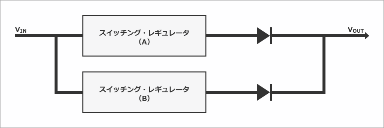
Diode OR connection
Some of you may be wondering, "Even if it's not a switching regulator that can be connected in parallel, it can be connected in parallel by configuring a diode-OR circuit as shown in Figure 2, right?"
This OR circuit is generally used when considering redundancy when one side of the power supply fails. It is thought that switching regulator (B) will continue to supply power even if switching regulator (A) on one side is broken. Therefore, if the regulator on one side is broken, it is designed so that one regulator can supply 100% load, so each switching regulator is used with a maximum load of 50%. Therefore, even if they are connected in parallel, the output capacity as a power supply circuit will not be doubled.
If you don't think about redundancy and think about maximizing output, you need to think about safety and create an external circuit with an On/Off function that turns the system off if one power supply fails. so be careful.
Furthermore, when a large amount of power is supplied, heat generation due to the loss of the diodes used in this OR circuit increases, so it is necessary to consider thermal design and the size of the diodes in the design.
Using a current balance control IC
There are control ICs that do not require troublesome current balance circuit design without worrying about diode loss.
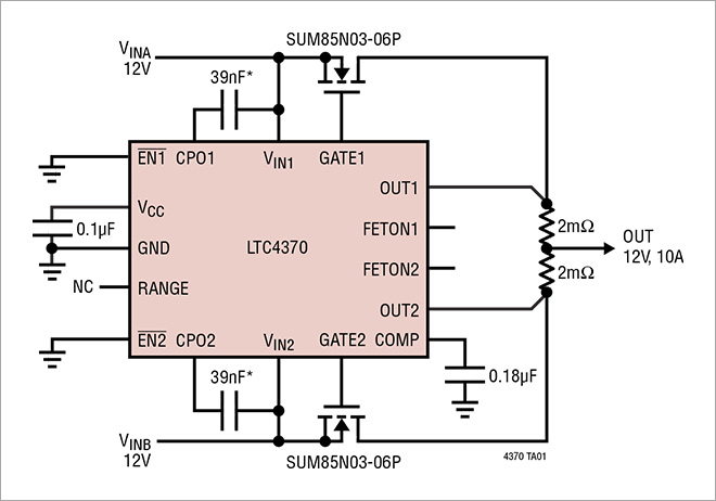
Parallel connection of switching regulators is possible by using Analog Devices' product LTC4370 (IC for diode OR circuit with current balance control).
Because the LTC4370 can use FETs instead of backflow diodes, power dissipation can also be very low. In addition, backflow prevention is also performed with FET in the same way as when using a diode.
With the circuit configuration shown in Figure 3, it is possible to obtain a total output of 12V/10A by connecting the switching regulator output of 12V/5A to VINA and VINB.
Use switching regulators that can be paralleled
Many analog devices switching regulators are parallelable. This time, we will introduce μModule products that are recommended for parallel connection and high power supply. When supplying a large amount of power, there is a high possibility of malfunction due to the board layout, so we recommend module products.
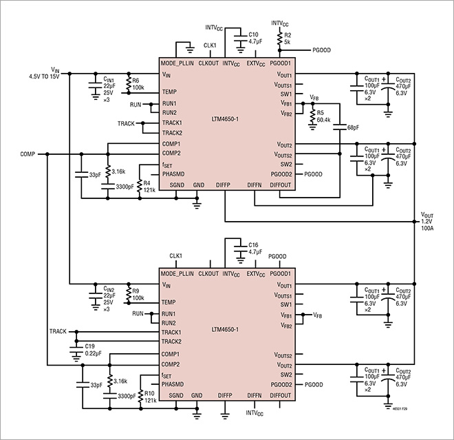
The LTM4650-1 is a two-channel 25A output in one package. This product can output 50A in one channel by combining the output of two channels. Figure 4 shows a configuration that can output 100A by connecting two modules in parallel.
The LTM4650-1 can parallel up to 6 modules for 300A output current.
Click here for recommended articles/materials
Solve analog circuit problems with μModule®!
How to reduce input switching noise in power supply design for board with FPGA?
Click here to purchase products
LTM4650AIY-1#PBF
Evaluation board for the LTM4650AIY-1
LTC4370IDE#TRPBF