- Semiconductor BusinessHOME
- Products and Services of Macnica,Inc.
-
technical information

-
Events and Seminars
- Handling Manufacturer
- Support
- Inquiry
- Click here to purchase products
- Semiconductor business e-mail magazine registration
![]()
![]() Narrow down by specifying conditions
Narrow down by specifying conditions
現在2168件がヒットしています。check

When using an FPGA with a large circuit scale, the amount of current that the FPGA requires from the power supply increases.
As a result, the RMS current flowing in the input line of the power supply increases.
As the input RMS current increases?
As the RMS current flowing into the input section of the DC/DC converter increases, the switching noise at the input section increases.
You may not have thought about the RMS current of your input before. However, if the current value used in the FPGA increases in the future, it will be necessary to confirm and consider.
Here, I would like to consider using the LTM4650A-1 DC/DC converter in Figure 1.
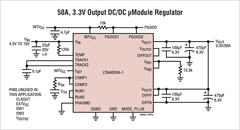
The LTM4650A-1 is a product containing two 25A output DC/DC converters.
It is possible to output 50A by making a single connection for 2 channels of DC/DC output.
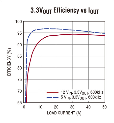
A high efficiency of about 95% is achieved even at 50(A) (Fig. 2).
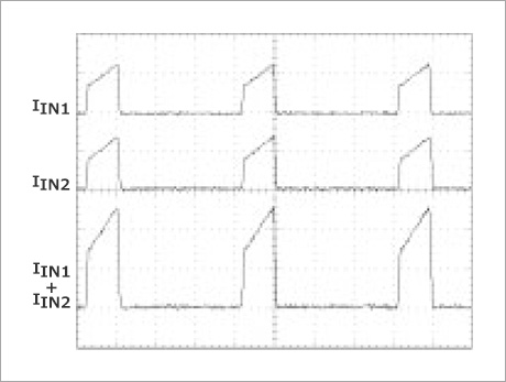
In general, the input RMS current for a single output looks like Figure 5.
The dual input currents IIN 1 and IIN 2 add together to form a large RMS current.
Large RMS currents appear as switching noise.
The noise from this RMS current can also cause the system to malfunction.
Calculate the RMS current using the following formula.
If the conditions are 12V input, 1.0V output, and 50A maximum current, the efficiency is about 87% from Figure 1.
The calculation yields an RMS current value of approximately 16A.
η%: Estimated efficiency of the power module
D: Buck Converter Duty Cycle
D = VOUT / VIN
Two-Phase Operation Reduces Noise Source RMS Current
Two-phase is an operation that shifts the switching timing of switching regulators 1 and 2 inside the LTM4650-1 by 180°.
As shown in Figure 4, regulator 1 input current IIN 1 and regulator 2 input current IIN 2 are 180° out of phase, doubling the frequency but keeping the maximum input current single phase. It's half the time it works.
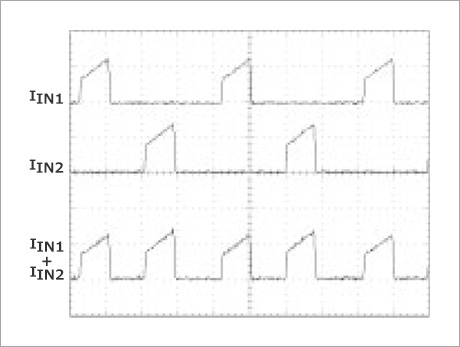
This reduces the switching noise that occurs in the input line, making it easier to take EMI countermeasures and reducing the effects of noise-induced system problems compared to single-phase.
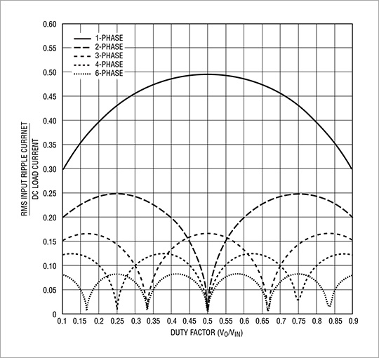
Estimate the two-phase RMS current from the normalized input RMS current graph in Figure 5. If Duty is approximately 0.1, the ratio of RMS/Maximum Current is 0.2.
The resulting RMS current for two-phase is about 10A, much less than the 16A for single-phase.
This greatly reduces switching noise appearing on the input lines.
Reduction of input ceramic capacitors
In addition to reducing input line switching noise, the reduced RMS current has another benefit.
It is possible to reduce ceramic capacitors.
In general, the self-heating of ceramic capacitors should be kept below 20°C.
Therefore, as the RMS current value increases, self-heating increases, so it becomes necessary to increase the number of capacitors to disperse the self-heating.
Suppose we were using a ceramic capacitor with an RMS current value of 4.2A that self-heated to 20°C.
Then the required number of ceramic capacitors for single and dual phase operation is:
- Single Phase: 4 (16A ÷ 4.2A = 3.81)
- Two-phase: 3 (10A ÷ 4.2A = 2.38)
Since an extremely large number of ceramic capacitors are mounted on an FPGA board, reducing the number of capacitors by even one is an advantage in manufacturing in terms of reducing implementation and management costs.