- Semiconductor BusinessHOME
- Products and Services of Macnica,Inc.
-
technical information

-
Events and Seminars
- Handling Manufacturer
- Support
- Inquiry
- Click here to purchase products
- Semiconductor business e-mail magazine registration


 Narrow down by specifying conditions
現在2240件がヒットしています。check


Hello, I'm Tott.
In the previous theoretical section, we explained that the reason why the data change points of an asynchronous counter occur at different timings for each bit is because the time it takes for the clock input to reach each register is different.
This time, I will explain that an asynchronous circuit is not suitable for FPGA design because the output timing of each register does not match.
Asynchronous circuits are not suitable for FPGAs! ! !
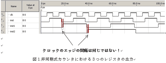
In the asynchronous counter, the clock input to each register uses the signal output from the previous stage register. Therefore, the edges of each clock may not have the same timing.
The cause of this clock edge difference is the wiring delay, as mentioned earlier.
Why Clock Edges Are Not Aligned
Route delays are compilation dependent on where the register generating the clock is placed on the FPGA device and which wires are used.
Since the delay due to the clock wiring between each register is not the same value, there is a difference in the change point of the output data.
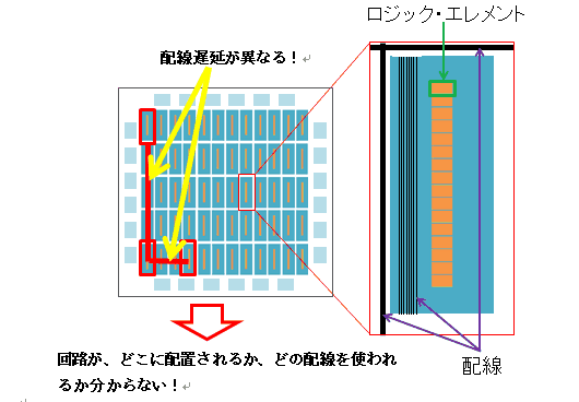
In the counter, the data change points are different when the clock edge driving each register is different.
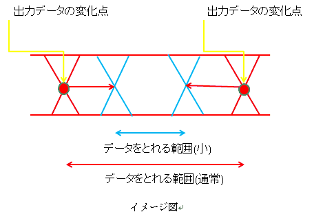
Different output data change points reduce the range of valid data and reduce the timing margin.
As a result, circuits that require high-speed operation may not be able to meet their timing constraints.
The faster the clock operating frequency, the more difficult it becomes to implement an asynchronous counter.
Conclusion
• Clock delay affects the circuit of an asynchronous counter.
- As the operating frequency of the clock increases, the delay of the asynchronous counter increases and it becomes impossible to meet the timing constraints.
・The clock delay of the asynchronous counter is not constant.
Therefore, I understood that an FPGA with a degree of freedom in placement and routing should be designed with a synchronous circuit.