- Semiconductor BusinessHOME
- Products and Services of Macnica,Inc.
-
technical information

-
Events and Seminars
- Handling Manufacturer
- Support
- Inquiry
- Click here to purchase products
- Semiconductor business e-mail magazine registration


 Narrow down by specifying conditions
現在2236件がヒットしています。check


Introduction
Hello. This is Totto, who feels every day that memory is deep.
Last time, we understood how DDR3 - SDRAM works.
This time, I wondered how DDR3 - SDRAM and FPGA interfaced, so I decided to investigate.
So I decided to ask the chief engineer of the senior engineer first.
Me: "FPGA and DDR3 - How does SDRAM interface with the FPGA?" 』
Headmaster: "Well, let's create a memory interface with MegaWizard Plug-In Manager first!" ! 』
Me : " ·····. 』
So I decided to ask the chief engineer of the senior engineer first.
For the time being, I decided to generate a memory interface as I was told.
When creating a memory interface...
I have a question on the screen below.
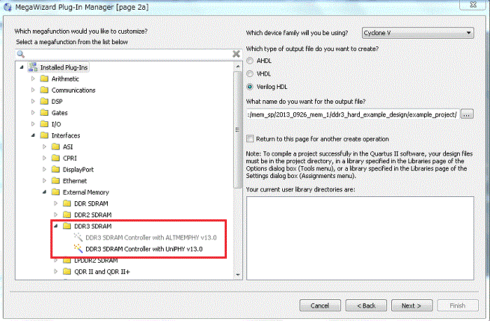
There are two types of memory interfaces, UniPHY and ALTMEMPHY.
So I decided to ask the chief engineer of the senior engineer first.
Me: "Which should I choose, UniPHY or ALTMEMPHY? 』
Headmaster: "What device are you using? 』
Me: “Cyclone® V. 』
Headmaster: ``Then it's UniPHY. 』
I managed to generate a memory interface without knowing what UniPHY is
Memory interface overview
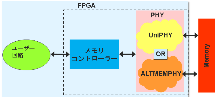
Me: ``Assuming that the controller controls the memory, what is UniPHY? I thought and looked into it.
What is PHY?
As shown in the image below, it is the part that first receives electrical signals from the memory, USB, Internet cable, etc. connected to the controller.
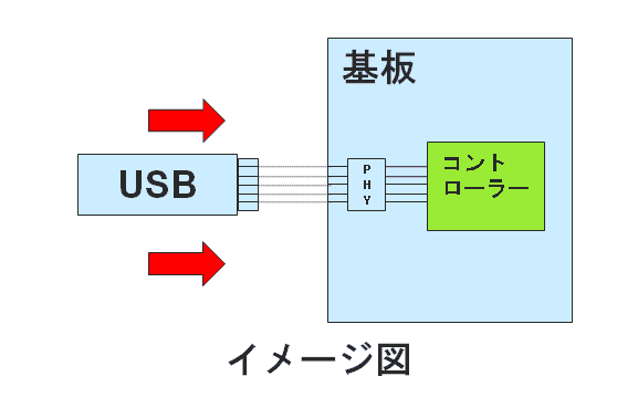
The PHY chip first physically receives electrical signals from USB, etc., and converts the electrical signals into digital data (1 , 0 ). (It also converts digital data into electrical signals.)
Altera's FPGA has a built-in PHY within the FPGA, and the part that first receives the electrical signal of the memory (DDR3 in this column) is UniPHY, ALTMEMPHY! I was convinced.
Summary of this time
・PHY is the part that first receives electrical signals from memory, USB, internet cable, etc.
・The PHY converts electrical signals to digital data (1, 0) and digital data (1, 0) to electrical signals.