- 半導体事業HOME
- マクニカの製品・サービス
-
技術情報

-
イベント・セミナー
- 取扱メーカー
- サポート
- お問い合わせ
- 製品購入はこちら
- 半導体事業のメルマガ登録


 条件を指定して絞り込む
現在2213件がヒットしています。check


はじめに
こんにちは。先輩エンジニアの頭領先輩に刺激を受け日々メモリについて学んでいるトットです。
今回はメモリの動作原理について書いていきます。
ライト ? リード ?
DDR3-SDRAM のライト、リード動作について、調べてみました。以下は、 DRAM の構造です。
DRAM のセルは、1つのトランジスタと1つのコンデンサからできています。
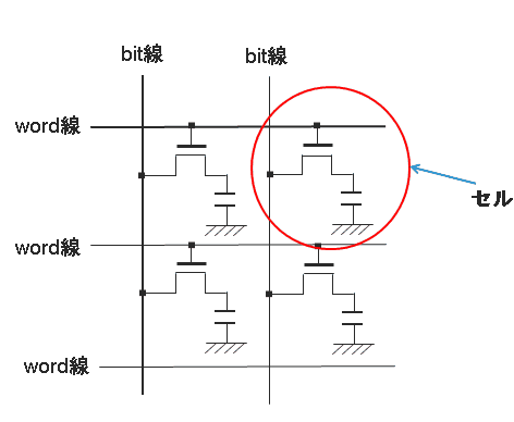
(注)上記の図はイメージ図です。
ライト
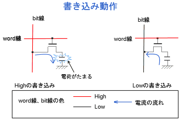
High の書き込み
1 . word 線、bit 線の電圧を High。
2 . bit 線の電圧を上げることにより word 線から電流が流れコンデンサに電荷がたまる。
Lowの書き込み
1 . word 線の電圧を上げ、bit 線をLowにし、コンデンサの電荷を放出し電荷がない状態にする。
リード
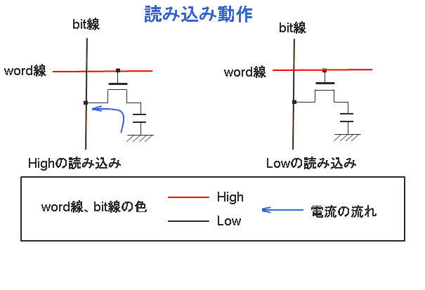
High の読み込み
1 . word 線を High、bit 線を Low の状態にする。
2 . コンデンサから電荷を放出することにより bit 線の電位が上がりHighと判別。
Low の読み込み
1 . word 線を High の状態にする。
2 . コンデンサには、電荷がないので電流は流れず bit 線の電圧に変化がなくLowと判別
小話
私 : 『 リフレッシュ動作ってなんですか ? 』
先輩 : 『 電池って放置しておくとどうなる ? 』
私 : 『 自然放電してしまいます。 』 と納得しました。
先輩 : 『 正解 ! 携帯の電池と同じようにコンデンサは、徐々に電荷が失われていくから、充電する必要があるんだよ。それがリフレッシュ動作だよ。 』
リフレッシュ動作は、セルのコンデンサを再充電することでデータを保持します。
メモリデバイスの動作については理解できたけど、メモリと FPGA はどのようにインタフェースをとっているんだろうと疑問に思った私は、調べてみることにしました。
今回のまとめ
■メモリとはデータを一時的に保存しておく場所。
■DRAM は、1 つのトランジスタと 1 つのコンデンサのセルからできている。