- Semiconductor BusinessHOME
- Products and Services of Macnica,Inc.
-
technical information

-
Events and Seminars
- Handling Manufacturer
- Support
- Inquiry
- Click here to purchase products
- Semiconductor business e-mail magazine registration


 Narrow down by specifying conditions
現在2217件がヒットしています。check

In this column, we will introduce "technical information on FPGA that is surprisingly unknown, but makes a difference if you know it."
From FPGA beginners to veterans, the contents can be used widely, so please keep in touch with us until the end.
[Lesson 6] How to reduce the load capacitance (C)
The low power consumption design method is an accumulation of detailed measures.
In order to understand the power consumption calculation formula, we will introduce typical low power consumption methods.
First, consider how to reduce the load capacitance “C” in the power consumption calculation formula.
In general, the load capacitance “C” is the sum of the “wiring capacitance” and the “pin capacitance of the input pin connected to the next stage”.
Reducing “C” not only reduces dynamic power, but also reduces leakage power due to the reduced resources.
To make it easier to visualize, if you compare the load capacity to a "bucket" and the electric charge to "water", when the bucket is filled with water from the hose, "H" will appear.
Suppose we empty the bucket and it becomes “L”.
There are two ways to fill all the buckets with less water: "reduce the number" of buckets and "decrease" the size of the buckets.
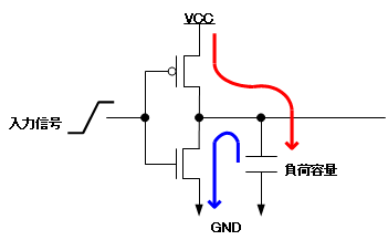
First, let's consider how to reduce the number of buckets, that is, how to reduce FPGA resources.
speed up and reduce parallelism
Running a circuit running at 500 MHz at 1 GHz cuts the data path width in half, saving a significant amount of resources.
Stratix ® 10, for example, doubles the performance of its predecessor with its HyperFlex architecture, which cuts circuit parallelism in half and saves resources.
Reduce ALM utilization
ALM (Adaptive Logic Module), which is the basic module of FPGA, consists of two ALUs for combinational circuits, an adder, a register, and so on. If the logic is the same, “C” can be reduced by reducing the number of ALMs used.
(a) Logic synthesis with Quartus ® Prime Pro's “area priority” reduces the ALU utilization.
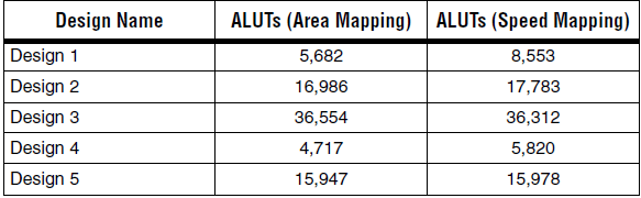
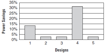
Since the maximum value of Fanout is fixed for FPGA, multiple ALMs may be used if the speed is increased.
Synthesize blocks that do not require speed with "area priority".
(b) Hard macro
It is possible to create memories and DSPs with ALMs for logic, but hard macros for memories and DSPs are optimized for the size and number of transistors, so “C” is much smaller.
Try to use dedicated hardware macros such as memory and DSP instead of ALM as much as possible.
(c) Power-Driven Synthesis
If the logic synthesis option makes the area extremely small, the number of toggles increases and power consumption may increase.
Quartus Prime's "Power-Driven Synthesis" prioritizes low power consumption for logic synthesis.
(d) Partial reconfiguration
Partial reconfiguration is a function that changes the circuit configuration of some blocks during operation.
By disconnecting circuits that are not in use, you avoid wasting power due to leakage power or clocks in that circuit.
(e) Reducing the number of ALMs by optimizing architecture and algorithms
When creating an algorithm, please be aware that the circuit scale will be small when designing.
Countermeasures during algorithm design are more effective than detailed low power consumption countermeasures after RTL completion.
(f) Adoption of fast (low speed grade) FPGA
Synthesizing on a faster FPGA may produce a smaller circuit than on a slower FPGA.
If logic synthesis is performed with an unreasonable performance requirement, a circuit with increased parallelism may be synthesized, so it is best to choose a device with a higher speed grade than a device with a larger area. There are cases.
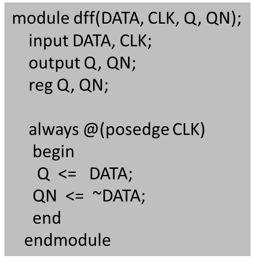
(g) Optimization of HDL description
The way HDL is written reduces the resources used.
For example, Verilog-HDL uses fewer "always" to reduce the number of registers, and more "don't cares" to reduce resources.
There are many other ways to optimize area by description.
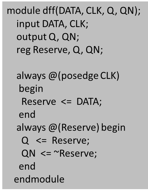
(h) code coverage
Use code coverage to find unused circuits.
If there are many specification changes, unnecessary circuits may be left behind, so use code coverage to search for unnecessary circuits and delete them.
Next is how to reduce the size of the bucket, that is, how to reduce the capacity.
Reduced capacity
(a) Nets with a high toggle rate are short
Since a large portion of FPGA power consumption is due to the wiring, nets with a high toggle rate should be wired as short as possible.
Nets with a high toggle rate between ALMs reduce wiring capacity when connected between ALMs within a Logic Array Block (LAB).
For example, if many circuits share common control signals such as enable and set, it becomes difficult to fit them within the LAB, so we try to minimize the number of control signals as much as possible.
That being said, it would be difficult to do it manually.
Quartus Prime's "Power-Driven Fitting" feature allows you to shorten wiring lengths by prioritizing nets with many toggles, and reduce power consumption by dividing memory. To maximize its effectiveness, please enter the toggle information as accurately as possible.
Partitioning wiring with many toggles so that it is located inside the block can be effective.
(b) Keep the wiring around the FPGA short.
Shortening the length of the wiring connected to the FPGA's output pins reduces the power consumption of the output buffer.
External load capacity is orders of magnitude larger than internal wiring capacity, so its impact is significant.
FPGAs offer a high degree of flexibility in pin placement, so pins are assigned in a way that minimizes wiring length, taking into account the location of surrounding devices.
(c) One-chip integration using FPGA
By incorporating functions previously handled by older process devices surrounding the FPGA into the FPGA itself, the wiring capacity and devices around the FPGA can be reduced. In particular, analog components should be digitized as much as possible.
FPGA processes are smaller and more power-efficient than peripheral devices, so power consumption can be lower than when implemented with older process devices.
Recently, by integrating the microcontroller surrounding the FPGA into a single device using Altera SoC FPGA, the wiring capacitance between the FPGA and the microcontroller is reduced, enabling high speed and low power consumption.
Furthermore, when performing high-speed communication, it is recommended to use the FPGA's built-in transceiver instead of placing SerDes outside the FPGA.
(d) Utilize Logic Lock
When using Logic Lock block-based designs, the wiring between blocks is often longer than the internal wiring within the blocks, so partition the blocks to minimize the number of toggles between them.
(e) Adoption of devices with fine processes
Miniaturized processes result in smaller transistors, which in turn reduces capacitance.
For the same circuit size, using devices with the latest miniaturized processes will result in lower power consumption.
Reduced pin capacitance
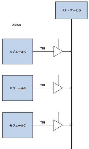
FPGAs and ASICs other than Altera may use tri-state buffers on their buses.
Because tri-state buffers have a very large input pin capacitance when closed, it is recommended to use a multiplexer (selector) instead of a tri-state buffer on the bus.
There are many other ways to reduce “C”.
Try to reduce the number of transistors used and shorten the wiring as much as possible.