- Semiconductor BusinessHOME
- Products and Services of Macnica,Inc.
-
technical information

-
Events and Seminars
- Handling Manufacturer
- Support
- Inquiry
- Click here to purchase products
- Semiconductor business e-mail magazine registration


 Narrow down by specifying conditions
現在2217件がヒットしています。check


In this column, we will introduce "technical information on FPGA that is surprisingly unknown, but makes a difference if you know it."
From FPGA beginners to veterans, the contents can be used widely, so please keep in touch with us until the end.
[Part 5] Is this the ultimate low power consumption method?
The low power consumption design method is an accumulation of detailed measures.
Rather than memorizing detailed measures, it is important to understand the power consumption calculation formula and the parameters used in it, and to design with an awareness of power consumption on a regular basis.
Until now, even if you thought it was troublesome to understand the calculation formula, we recommend that you take a look at the calculation formula once.
I think you can get a quicker understanding by looking at which parameters the low power techniques you know affect.
1.1 Power Consumption Calculation Formula for CMOS Circuits
| power consumption | = | dynamic power + leakage power |
| = | [switching power + short circuit power] + leakage power | |
| = | [0.5*(C*Vs*VCC*F)*N] + [Q*VCC*F*N] + [(Idc+Ileak)*VCC] |
| C: load capacity |
| Vs: signal amplitude |
| VCC: power supply voltage |
| F: operating frequency |
| N: Signal transition frequency (toggle rate) |
| Q: Charge due to through current |
| Idc: circuit-specific DC current |
| Ileak: Leak current |
1.1.1 Dynamic power
The power at which the signal transitions, which is the sum of the switching power and the short-circuit (through) power.
(1) Switching power
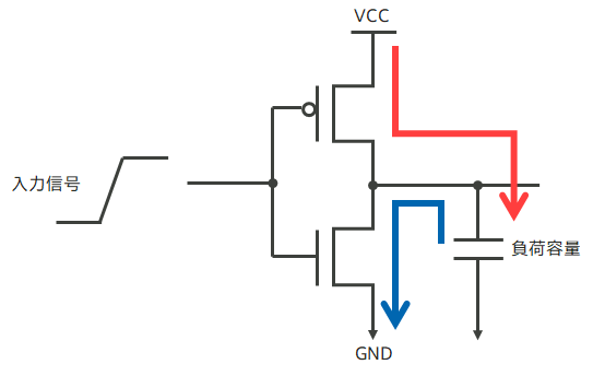
It is the power consumed when the cell operates and charges and discharges the load capacity.
The load capacitance is the sum of the wiring capacitance and the input pin capacitance of the next cell.
For example, inputting “L” to the inverter input turns pMOS “ON” and nMOS “OFF”, and current flows from VCC to charge the wiring and the capacitance of the input pin of the next stage. At this time, power is consumed by the pMOS resistance.
Next, when “H” is input to the input of the inverter, the pMOS becomes “OFF”, the nMOS becomes “ON”, and the charge charged in the load capacitance flows to GND through the nMOS. At this time, power is consumed by the nMOS resistance.
This capacitance is the sum of the wiring resistance and the input pin capacitance of the next-stage cell, and the longer the wiring and the larger the fanout, the greater the switching power.
(2) Short circuit power
In CMOS, if the input signal is stable at ``L'' or ``H'', either pMOS or nMOS will always be OFF, and no current will flow from VCC to GND except for leakage current.
This is why CMOS is said to have low power consumption. However, if the rise or fall of the input signal is slow, both the pMOS and nMOS will be in the ON state where they are slightly open temporarily.
At this time, a short-circuit current flows from VCC to GND, and this power is called short-circuit power.
1.1.2 Leakage power
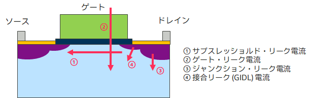
Leakage power is the power transmitted by the following four types of leakage currents.
While the old process had a negligible value, the newer process had significantly higher leakage power.
These leakage powers are consumed regardless of operation if voltage is applied to the transistor.
Subthreshold leakage current and gate leakage current dominate today.
Since the subthreshold leakage current is highly dependent on temperature, leakage power increases further at higher temperatures.
|
kinds |
Contents |
Cause |
Temperature Dependence |
| Subthreshold leakage current (source-drain leakage) |
Current that flows between the source and drain when the transistor is in the OFF state | Vt (threshold voltage) drop of transistor |
Big |
| Gate leakage current | Due to the tunnel effect, current flowing from the gate through the gate oxide to the source |
Thinner gate oxide film |
small |
| Junction leakage current | Current flowing between source, drain and substrate | Increased concentration of impurities and Element crystal defects, etc. |
small |
| Junction leakage (GIDL) current | Current due to electric field between gate and drain | Thinner gate oxide film |
small |
Table 1. Leakage Current Comparison
From the next time, we will introduce specific methods for reducing each parameter.