- Semiconductor BusinessHOME
- Products and Services of Macnica,Inc.
-
technical information

-
Events and Seminars
- Handling Manufacturer
- Support
- Inquiry
- Click here to purchase products
- Semiconductor business e-mail magazine registration


 Narrow down by specifying conditions
現在2222件がヒットしています。check

In this column, we will introduce "technical information on FPGA that is surprisingly unknown, but makes a difference if you know it."
From FPGA beginners to veterans, the contents can be used widely, so please keep in touch with us until the end.
[Part 3] Is this leak power? "No, it's DC power."
If you check the circuits that are said to have large leakage power, there are many cases where the cause is DC power.
Considering DC power in circuit design helps reduce standby power consumption, so this time I will explain DC power.
CMOS circuitry is a low power process
CMOS circuits are said to be low power processes because either pMOS or nMOS is closed when not in operation, and no DC current flows from Vdd to GND.
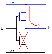
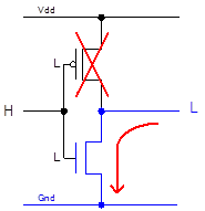
However, even in CMOS circuits, a DC current flows when a pull-up or pull-down is performed. This is DC power.
For example, FIG. The output buffer with pull-up has a pull-up resistor on the Vdd side.
Inputting “H” turns the upper transistor “OFF” and the lower transistor “ON”, connecting the output pin and GND.
Although the upper transistor is OFF, there is a pull-up resistor in parallel, so DC current flows from Vdd ⇒ Pull-up resistor ⇒ Gnd along the red arrow in Figure 3.
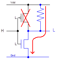
DC power consumes "V 2 /R" power with only one pull-up resistor, and power consumption increases when the resistance value is reduced.
Similarly, a pull-down has a resistor between the output pin and GND, so it will consume DC power when the output is high.
Therefore, standby power consumption can be reduced by increasing the resistance value, such as pulling up when the “H” state is long and pulling down when the “L” state is long.
If you look at a design with large leakage power, please be aware that there are cases where DC power is wasted without paying attention to pin processing.
Before suspecting leak power, check the DC power first.