- Semiconductor BusinessHOME
- Products and Services of Macnica,Inc.
-
technical information

-
Events and Seminars
- Handling Manufacturer
- Support
- Inquiry
- Click here to purchase products
- Semiconductor business e-mail magazine registration


 Narrow down by specifying conditions
現在2232件がヒットしています。check

In this column, we will introduce "technical information on FPGA that is surprisingly unknown, but makes a difference if you know it."
From FPGA beginners to veterans, the contents can be used widely, so please keep in touch with us until the end.
[Lesson 2] Is clock gating (gated clock) effective?
Clock gating (hereafter abbreviated as CG) stops the clocks of registers that do not have data changes to reduce the power consumption of the clock network and
It is a technique to reduce the power consumption of the registers and gates connected to it.
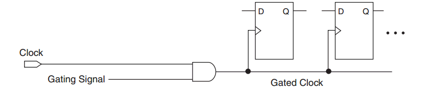
As shown in Figure 1, put a gate such as AND in the clock to stop the clock.
Designers often ask, "Can we use CG on FPGAs?"
The answer is that you can use CG on FPGA as well.
However, Fig.1. It is not recommended to stop the clock by inserting AND etc. into the clock network as in .
Use Intel's CG-only block “ALTCLKCTRL” to stop the clock.
In fact, even in ASIC, CG is prohibited in the user circuit, and a dedicated CG cell synchronized with the clock is used.
Fig.1. There is a possibility that glitches may occur due to the timing of the signal and clock of “Gating Signal” of
This is because the skew between the AND and the subsequent register cannot be guaranteed.
Before that, when you put a gate on the clock line, it becomes an asynchronous circuit, so many EDA tools cannot handle it.
By using the CG dedicated cell, the EDA tool can treat the CG dedicated circuit as a synchronous circuit by replacing it with the data enable circuit and recognizing it.
There are two main ways to do CG.
(1) How the tool automatically CG
(2) How designers intentionally stop the clock
How the tool automatically CG
Stops the clock when the F/F is disabled when there are multiple F/Fs sharing the clock with the enable.
The F/F does not operate when there is no data transition, and the power consumption of clocks including MUX can be reduced.
Placing the CG dedicated circuitry as close to the root of the clock as possible also reduces the power consumption of the clock tree.
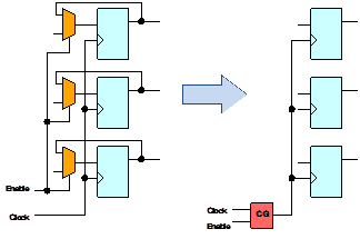
In ASIC, clock power accounts for a high percentage of total power consumption, so automatic CG is effective, but
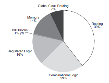
In FPGAs with different structures, the clock power accounts for only a few percent, so it is not very effective.
How Designers Intentionally Stop Clocks
This is a method for stopping the clock of circuits that do not need to be running.
Since FPGAs consume a large portion of their total power through I/O and wiring, this method is more time-consuming than (1), but it is more effective.
However, since the tool cannot determine where to stop the clock, the designer must intentionally stop the clock for the block.
For the circuitry connected to the clock line, please use the CG-specific block "ALTCLKCTRL" provided by Altera.
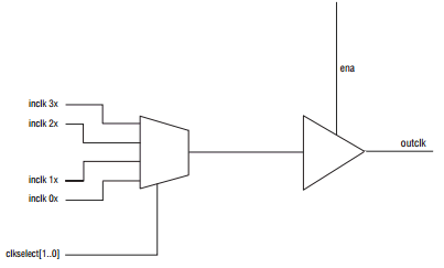
Click the URL below to automatically download the “ALTCLKCTRL” document (PDF).
Clock Control Block (ALTCLKCTRL) IP Core User Guide