- Semiconductor BusinessHOME
- Products and Services of Macnica,Inc.
-
technical information

-
Events and Seminars
- Handling Manufacturer
- Support
- Inquiry
- Click here to purchase products
- Semiconductor business e-mail magazine registration
Product Summary
CrossLink-NX is a device built on 28 nm FD-SOI technology, a platform for next-generation Lattice FPGAs. By adopting FD-SOI, it is possible to achieve higher reliability and lower power consumption than ever before. CrossLink-NX incorporates two MIPI D-PHYs as hard blocks and can support data rates up to 2.5Gbps per lane.
Differential I/Fs such as LVDS, SLVS, and subLVDS other than MIPI I/F support up to 1.5 Gbps per lane, and the built-in hard block for PCI Express (Gen1, Gen2) is the first generation It is possible to support interfaces in various fields than CrossLink™. Logic capacity is also up to 39K logic cells, 56 18x18 multipliers, 2.9 Mb embedded memory (consisting of EBR and LRAM blocks), 12bit ADC, DRAM interface (supports DDR3, DDR3L, LPDDR2, LPDDR3, up to 1066 Mbps) This is a product with dramatically improved functions compared to the original CrossLink™.
In addition, we provide a large number of IP (Intellectual Property) modules for CrossLink-NX, and it is possible to configure the IP on the GUI according to the customer's specifications. Using these IPs eliminates the need for language-based design, making it possible to significantly reduce design man-hours.
Hardware and functions installed in the product
FD-SOI
CrossLink-NX uses 28nm process FD-SOI, a next-generation architecture. By adopting FD-SOI, it is possible to improve the system for soft errors by approximately 100 times compared to conventional products and achieve low power consumption (up to 75% lower power consumption than other companies' products in the same scale range). increase. In addition, it is possible to change the bias inside the device programmably, and it is possible to switch between a low power consumption version and a high performance version in the same device.
MIPI D-PHY
CrossLink-NX contains two MIPI D-PHY as hard blocks and supports data rate of 2.5Gbps per lane.
Since one MIPI D-PHY block supports up to CLK 1lane and Data 4lane, it is possible to support data rates up to 10.0Gbps with one MIPI D-PHY block. In addition, since it supports both MIPI CSI-2 and MIPI-DSI, it enables a wide range of I/F bridges on the camera interface side and display interface side.
Programmable I/O
CrossLink-NX provides programmable I/O that can be set to support various I/Fs other than MIPI I/F. Specifically, it is possible to support various I/Fs such as LVDS (Rx, Tx), Sub-LVDS (Rx), HiSPI (Rx), SLVS200 (Rx, Tx), and LVCMOS. These I/Os support data rates up to 1.5Gbps/lane when using differential I/F.
EBR (Embedded Block RAM)
CrossLink-NX has a built-in memory made up of hard blocks called EBR. With a maximum capacity of 1512kbit, it is possible to configure functions such as a simple data buffer without using the user logic area.
LRAM
CrossLink-NX has a built-in large-capacity memory block called LRAM in addition to EBR. With a maximum capacity of 2560 kbit, it is possible to handle cases where a certain amount of memory capacity is required, such as configuring a line buffer without using an external memory.
I2C, SPI hard block
CrossLink-NX has built-in I2C and SPI hard blocks and can be configured via I2C and SPI. If the host CPU and SoC are mounted on the board, it is possible to configure via I2C and SPI using these hard blocks without external FLASH. It also supports Quad SPI, enabling configuration in the order of tens of milliseconds.
PCI-Express block
CrossLink-NX has a built-in PCI-Express (Gen1, Ge2) hard block, enabling it to support interfaces in a wider range of fields than ever before.
DSP block
CrossLink-NX has a built-in DSP for arithmetic processing. With up to 56 built-in 18 X 18 Multipliers, it is possible to implement necessary arithmetic processing without consuming the user logic area, such as image processing as well as video signal bridging.
ADC
It has 2 channels of 1 MSPS, 12-bit SAR ADC. This makes it possible to process analog signals from sensors, monitor supply voltages, and more.
DRAM interface
CrossLink-NX supports DRAM I/F (DDR3, DDR3L, LPDDR2, LPDDR3 supported, maximum 1066 Mbps). This makes it possible to construct a frame buffer, which is necessary for image processing, etc.
Example of product use
The figure below is just an example, so please feel free to contact us from the inquiry button at the bottom of this page regarding feasibility.
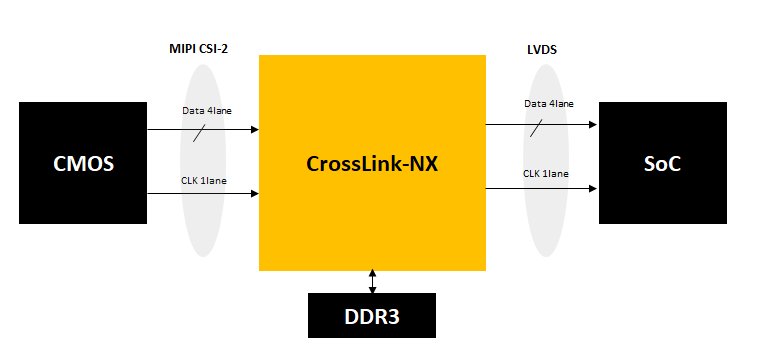
Usage example 1
・This is an example of use in a case where the MIPI I/F output from the CMOS sensor cannot be directly connected to the subsequent SoC.
・It is assumed that a frame buffer will be built using DDR3 memory and image processing will be performed using the internal DSP.
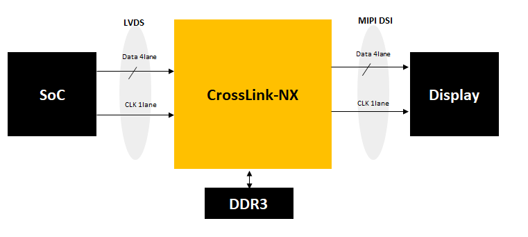
Usage example 2
・This is an example of use when the SoC and Display cannot be directly connected. .
・It is assumed that a frame buffer will be built with DDR3 memory and image processing will be performed by the internal DSP.
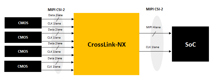
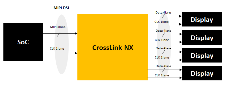
Usage example 3
This is an example of use in a case where multiple channels of MIPI signals input from a CMOS sensor cannot be connected because the MIPI port of the subsequent SoC is only 1ch.
Usage example 4
This is an example of use in a case where MIPI signals cannot be connected to multiple displays in the subsequent stage because the previous stage SoC has only one MIPI port.
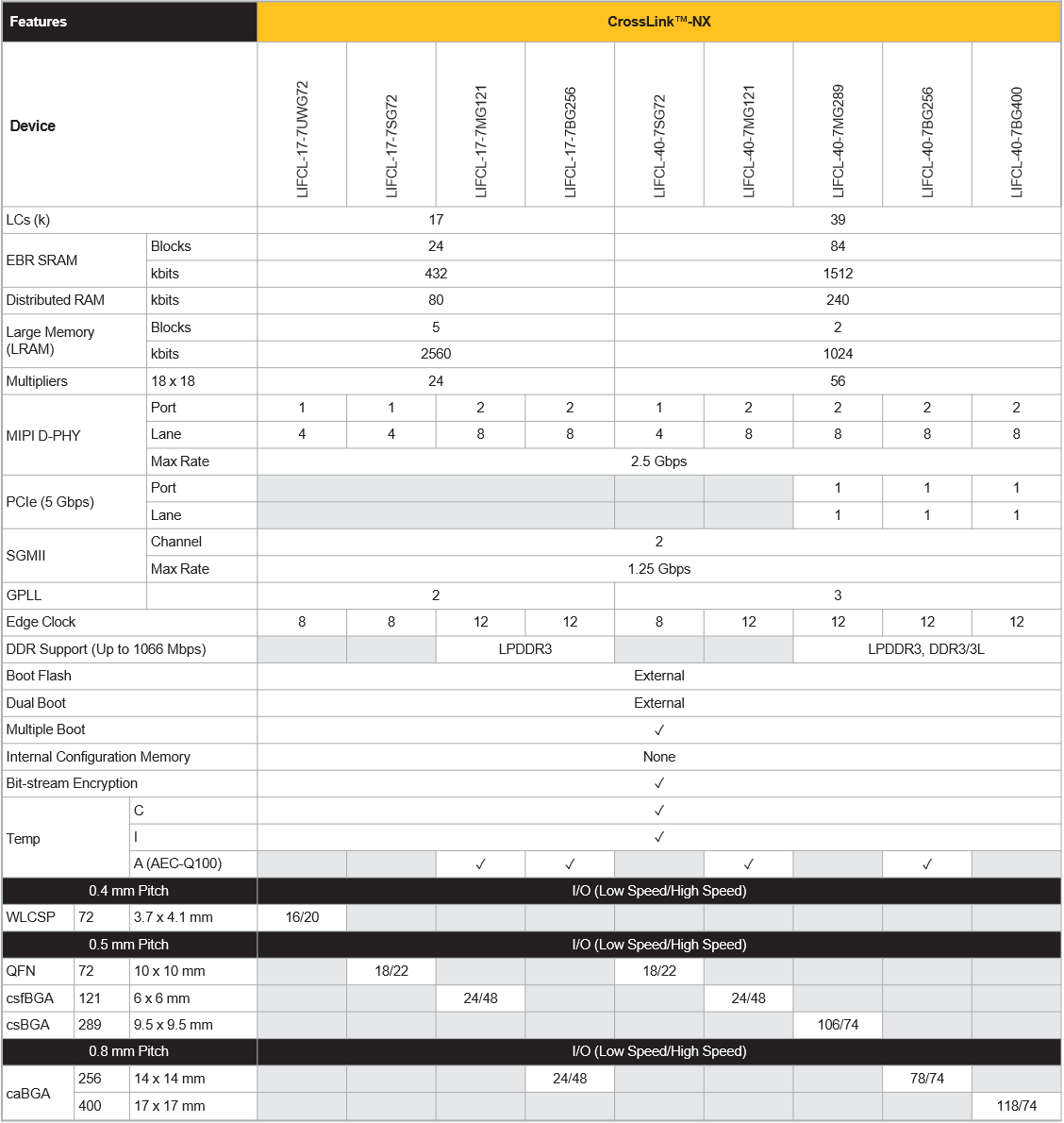
Package lineup
Inquiry / Quotation
If you have any questions or requests for quotations regarding this product, please contact us using the form below.
Design Tool Information
The design tool for CrossLink NX is "Radiant".