- Semiconductor BusinessHOME
- Products and Services of Macnica,Inc.
-
technical information

-
Events and Seminars
- Handling Manufacturer
- Support
- Inquiry
- Click here to purchase products
- Semiconductor business e-mail magazine registration
Product Summary
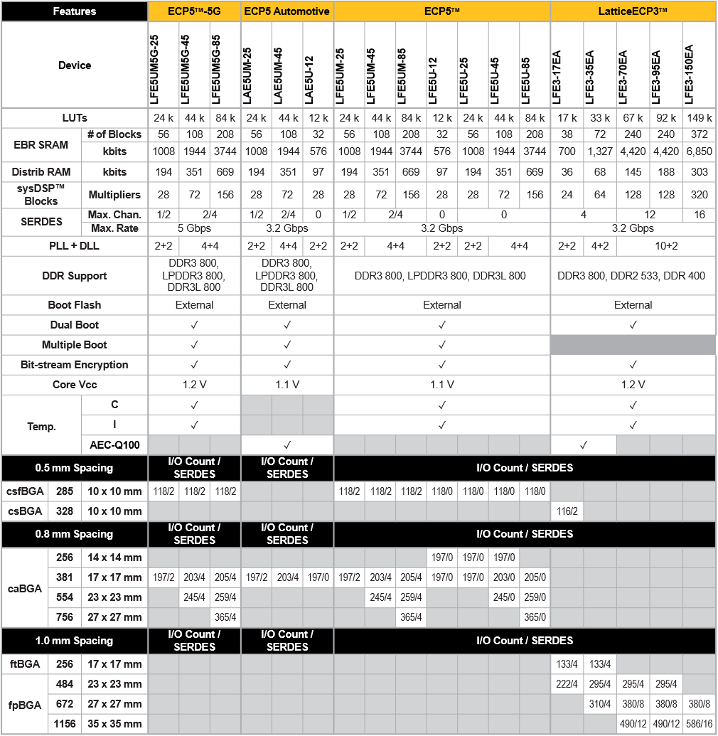
The ECP5 has a maximum logic capacity of 85K, 3.7Mbit EBR memory, a DSP block for arithmetic processing, and a high-speed memory interface including 800 Mbps DDR3. Furthermore, ECP5 can support high-speed I/F such as PCIExpress Gen2, Ethernet, and V-by-One with MAX5.0Gbps low power consumption SERDES core.
ECP5 has been released from 285 csfBGA (10 x 10mm) type to 756 caBGA multi-pin type and AEC-Q100 compliant automotive products, so it can be used in a wide range of fields and applications. Compared to other companies' FPGAs of the same size, it excels in low power consumption, and can offer advantages in a wide range of fields and products, such as reducing the heat dissipation mechanism and downsizing.
In addition, Lattice provides various AI solutions as devices for Lattice edge AI solutions, taking advantage of the features of the ECP5, which incorporates a DSP and memory of up to 3.7Mbit into a low-power, small-package FPGA. For more information about Lattice Edge AI solutions, please feel free to contact us.
Features of installed hardware and functions
SERDES block
The ECP5 has an integrated SERDES block that can support data rates up to 5.0Gps. This makes it possible to support high-speed serial interfaces such as PCIExpress Gen2, Ethernet, and V-by-One.
DSP block
The ECP5 has a built-in DSP for arithmetic processing. Since a maximum of 156 18 X 18 Multipliers are built-in, it is possible to realize the necessary arithmetic processing without consuming the user logic area, such as performing not only video signal bridging but also image processing.
DRAM interface
ECP5 supports DRAM I/F (DDR2/DDR3 and LPDDR2/LPDDR3, up to 800 Mbps). This makes it possible to configure a frame buffer that is necessary for image processing, etc.
EBR (Embedded Block RAM)
The ECP5 has a built-in memory made up of hard blocks called EBR. With a capacity of 3.7Mbit, it is possible to configure functions such as a simple data buffer without using the user logic area.
Programmable I/O
ECP5 supports clock parallel high-speed differential I/F and single-ended I/F such as LVCMOS, LVDS, Sub-LVDS (Rx), and MIPI (Rx, Tx).
ECP series package lineup
Inquiry / Quotation
If you have any questions or requests for quotations regarding this product, please contact us using the form below.