- Semiconductor BusinessHOME
- Products and Services of Macnica,Inc.
-
technical information

-
Events and Seminars
- Handling Manufacturer
- Support
- Inquiry
- Click here to purchase products
- Semiconductor business e-mail magazine registration
CrossLink™ series product overview
CrossLink™ is a programmable device that supports various I/F bridges. It is a MIPI D-PHY built-in type FPGA with strengths of low power consumption, low cost, and small package.
CrossLink™ supports video I/F such as MIPI CSI-2, MIPI DSI, OpenLDI, SLVS200, SubLVDS, HiSPi.
Lattice Semiconductor provides a large number of IP (Intellectual Property) modules for CrossLink™, and it is possible to configure the IP on the GUI according to the customer's specifications. Using these IPs eliminates the need for language-based design, making it possible to significantly reduce design man-hours.
CrossLink™ is not only used in consumer products such as smartphones, tablets, wearables, VR, AR, drones, smart homes, and HMI, but also in the industrial equipment field, as well as in-vehicle products that have acquired AEC-Q100 certification. Various bridging solutions for the market are also available.
CrossLink™ series product features
About installed hardware and functions
MIPI D-PHY
CrossLink™ contains two MIPI D-PHY as halves and supports data rate of 1.5Gbps per lane.
Since one MIPI D-PHY block supports up to CLK 1lane and Data 4lane, it is possible to support data rates up to 6.0Gbps with one MIPI D-PHY block.
In addition, since it supports both MIPI CSI-2 and MIPI-DSI, it enables a wide range of I/F bridges on the camera interface side and display interface side.
Programmable I/O
CrossLink has I/O that can be programmed and set to support various I/Fs other than MIPI I/F.
Specifically, it is possible to support various interfaces such as LVDS (Rs, Tx), Sub-LVDS (Rx), HiSPI (Rx), SLVS200 (Rx), and LVCMOS. These I/Os support data rates up to 1.2Gbps/lane when using differential I/F.
user logic
The user logic size of the SRAM structure is 6K LUTs. Therefore, it is possible to implement functions other than the I/F bridge in the remaining user logic area, or to integrate peripheral logic ICs.
Embedded Block RAM (EBR)
CrossLink has built-in memory made up of hard blocks called EBR.
With a capacity of 180kbit, it is possible to configure functions such as a simple data buffer without using the user logic area.
I2C, SPI hard block
CrossLink™ has built-in I2C and SPI hard blocks and can be configured via I2C and SPI.
If the host CPU and SoC are mounted on the board, it is possible to configure via I2C and SPI using these hard blocks without external FLASH.
Power Management Unit
CrossLink™ has a built-in hard block called Power Management Unit that can be put into sleep mode to reduce power consumption.
By using this hard block, it is possible to reduce the power consumption during sleep to the uW order level. It is possible to provide benefits for mobile applications and battery-powered applications.
Example of use
The figure below is just an example, so please feel free to contact us from the inquiry button at the bottom of this page regarding the feasibility.
Example of use in cases where the MIPI I/F output from the CMOS sensor cannot be directly connected to the subsequent SoC
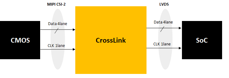
*The number of lanes and the CrossLink output side I/F (LVDS) in the above diagram are just examples.
Usage example when SoC and Display cannot be directly connected
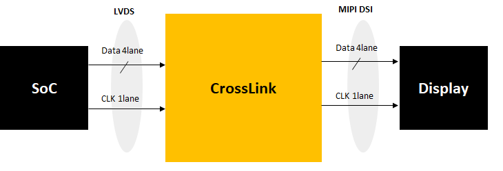
The number of lanes in the diagram above and the input side I/F (LVDS) of CrossLink are just examples.
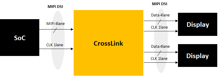
Example of use in a case where MIPI signals cannot be connected to the two displays in the latter stage because the MIPI port of the previous stage SoC is only 1ch.
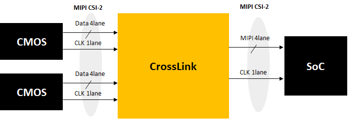
Example of use in a case where MIPI signals cannot be connected to the two displays in the rear stage because the front stage SoC has only one MIPI port.
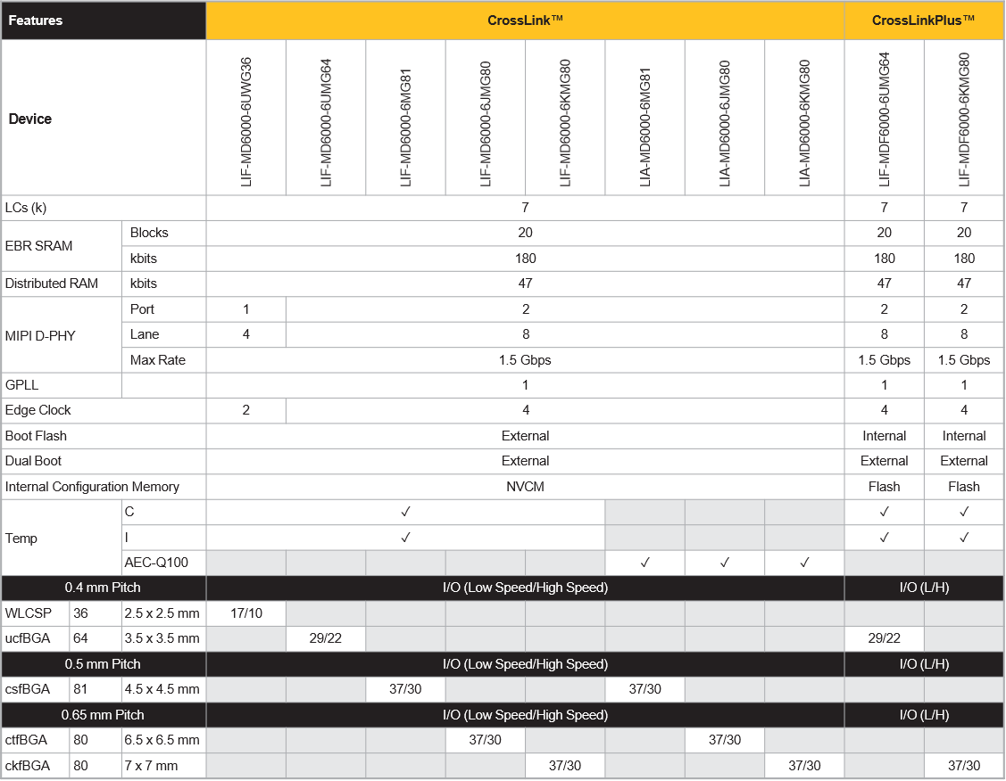
CrossLink™ series package lineup
Inquiry / Quotation
If you have any questions or requests for quotations regarding this product, please contact us using the form below.