- Semiconductor BusinessHOME
- Products and Services of Macnica,Inc.
-
technical information

-
Events and Seminars
- Handling Manufacturer
- Support
- Inquiry
- Click here to purchase products
- Semiconductor business e-mail magazine registration

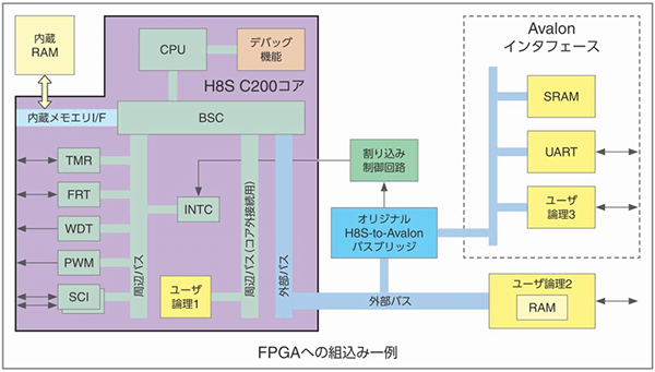
Equivalent to Renesas Electronics H8S C200
Features
- Instruction set compatible with H8S family standard microcontroller products
- The built-in memory I/F can connect up to 256 Kbytes of Intel FPGA compiled memory.
- User logic can be connected to peripheral bus (for connection outside core) and external bus
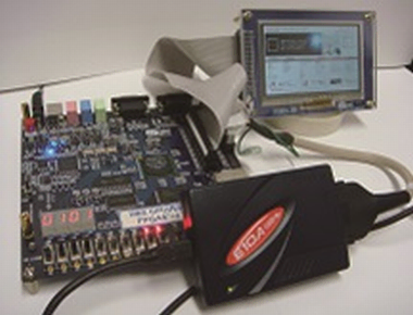
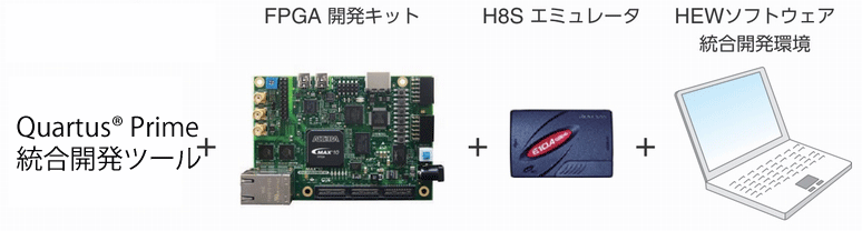
- Debug function enables on-chip debugging by using the E10A-USB emulator
Why FPGA IP cores?
- Achieving a platform and CPU for high-mix, low-volume applications
- Customize the peripherals required for each device by changing the FPGA circuit
- Discrete product discontinuation countermeasures
- User-original CPU design is possible
- Easy porting of software from existing H8S C200
- レジスタコンパチ品となりますので、ソフトウェアの検証工数をミニマイズ
Development environment
H8S C200 core/figure embedded image
- FPGA enables the realization of a customer-original microcomputer-equipped system chip.
- Customer-owned IP can be incorporated into the internal peripheral bus
- Internal memory (each RAM, ROM) can be up to 256KB by using FPGA's compile memory function (each RAM, ROM).
- With many external interrupts, there is a degree of freedom in interrupts not found in standard products.
Offerings
- Cryptographic RTL (Verilog HDL)
- User's Manual