- Semiconductor BusinessHOME
- Products and Services of Macnica,Inc.
-
technical information

-
Events and Seminars
- Handling Manufacturer
- Support
- Inquiry
- Click here to purchase products
- Semiconductor business e-mail magazine registration
![]()
![]() Narrow down by specifying conditions
Narrow down by specifying conditions
現在2189件がヒットしています。check
Consumer demands and key takeaways are constantly changing. Users of mobile and computing devices are constantly looking for smaller, lighter and more sophisticated products, demanding more features and better performance. Applications that were once required on laptops have migrated to smartphones, and applications that were only available on smartphones are now supported by smartwatches.
Designers continue to evaluate new ways to meet the ever-increasing demand for miniaturization. One of the top priorities in doing so is system storage. Using serial NOR flash memory used for code storage and serial NAND flash memory used for data storage and code backup occupies a relatively large footprint in space-limited designs will be
Winbond is the world leader in serial NOR and serial NAND flash IC production volume, with extremely fast read/write operations between flash memory and host and system-on-chip (SoC), microprocessors and microcontrollers. He helped solve this problem by inventing the Quad Serial Peripheral Interface (QSPI), a high-bandwidth version of the standard serial peripheral interface that allows
Winbond's QSPI matches the data slew rate of parallel flash with far fewer channels and a smaller package, making this innovation an important step in reducing the memory footprint on system boards.
In recent years, serial flash manufacturers have also adopted a method of increasing memory capacity while reducing footprint by stacking flash memory dies within a single package.
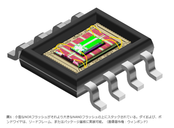
This article outlines the impact of replacing multiple flash memory ICs with a single stacked die package and how the new stacked die technology developed by Winbond outperforms other solutions. , and how the pin count and footprint have been reduced.
Advantages of Stacked Die
A typical flash memory use case in a small device design consists of a 16Mbit serial NOR flash device for code storage and a 1Gbit serial NAND flash device for data and the Linux operating system. NOR flash offers excellent random access performance, endurance, retention, and other important features for storing frequently read code. NAND flash offers faster programming and is cheaper than NOR flash at densities above 512Mbits. The read latency is longer, but given the infrequent data access, this is acceptable.
A typical system design requires two flash memory packages to be implemented on the board, each with its own SoC interface.
In this use case, the footprint can be easily reduced by using a stacked die package (see Figure 1). In a heterogeneous package, a small NOR flash is stacked on top of a larger size NAND flash die.
Similar benefits can be achieved with homogeneous packages such as stacking NOR on top of NOR or NAND on top of NAND. For example, if an existing product design using 512Mbit NAND flash requires additional data capacity, the traditional approach would be to replace the 512Mbit IC with a 1Gbit version. However, a different footprint and pinout for a 1Gbit device would take a long time to redesign the board.
Homogeneous packages save this board design effort. Two stacked 512Mbits can be housed in the same package with the same pinout as a single 512Mbit die, so you can instantly double the memory capacity without redesigning the board.
The two advantages of not having to recreate the board footprint and reducing development resources are unique to the stack die concept.
Winbond has introduced a new stacked-die approach in flash memory. This further significantly reduces the board footprint while improving read/write performance.
Low pin count stacked package
One of the major challenges in implementing stacked-die products is providing an interface between the SoC or microcontroller and the two (or more) dies in the flash memory package. To avoid contention on the SPI bus, the SoC uses the Chip Select (CS) command to tell the stacked package which die is valid as an interface.
Other stacked memory solutions implement this CS function in hardware via dedicated CS lines (one for each die). So a package with 2 dies has 2 CS lines and a package with 3 dies has 3 CS lines.
Clearly, this is an inconvenient situation given the increased pin count of memory devices and SoCs, as well as the need for more wiring on the board.
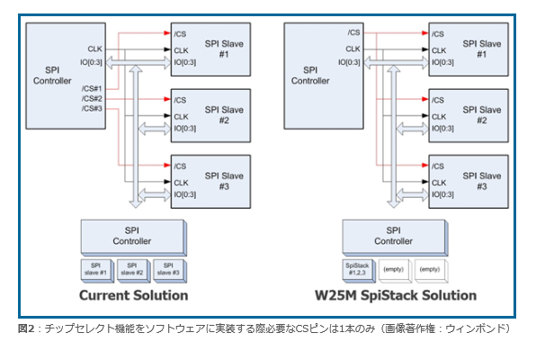
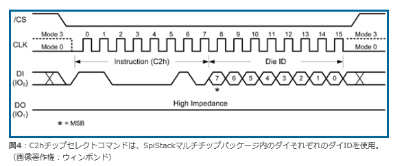
Winbond's new W25M SpiStack flash memory product solves this problem by using a software chip select function that allows a single CS channel between the memory device and the SoC (see Figure 2). Each die contained in a SpiStack package has a die ID, and a simple chip select command and associated die ID is used to tell all the dies which chips in the SpiStack package use the SPI bus.
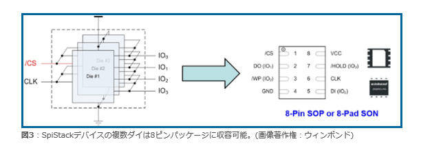
This software CS function operates through only a single CS pin on the memory device or SoC and requires only one CS wire between them. The reduced pin count allows as many as 2 to 4 die in a standard 8-pin SO, or 8-pad SON package. Stacked die implementations that use the hardware CS feature are typically 16-pin SOs or 24-ball BGAs and require larger and more complex board designs (see Figure 3).
It is easy for designers to integrate the SpiStack's CS functionality into their system software. The C2h command is used to select any die within the flash memory package (see Figure 4). C2h commands can be issued at any time to change the active die, regardless of die activity. Only one selected die is active on the SPI bus.
Speedy read/write operations
Flash memory inherently takes longer to program than SRAM or DRAM. When using single-die flash, it often happens that the system reads the memory in the middle of a write. Then the controller must first issue a write suspend command, then a memory read command, then a write resume command. Complicated use of flash memory slows down read and write processes.
Winbond removes this bottleneck by introducing a new concurrency feature in its SpiStack product. The SoC can perform write and erase operations while one die in the SpiStack product is performing a read operation from a different die (see Figure 5).
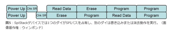
As mentioned above, only one die can have access to the SPI bus at any given time, but the SpiStack device allows multiple dies to perform write, read, and erase operations simultaneously.
For many applications, this memory concurrency feature can greatly improve the speed of operations. In other words, SpiStack devices enable faster operation than comparable devices that run only in sequential mode.
Abundant product lineup of the same and different types
SpiStack multi-die packages are available in NOR+NAND heterogeneous configurations, NOR+NOR and NAND+NAND homogeneous configurations, each with a wide variety of package types and densities. As the world's largest serial flash manufacturer, Winbond offers system designers a wide range of memory densities and package options.
It allows flexibility in design and allows replacement of devices with a common footprint and pinout to meet changing memory density requirements.
Some examples of SpiStack devices for sale are:
- 16Mbit NOR + 1Gbit NAND
- 512Mbit NOR (256Mbit NOR x 2)
- 2Gbit NAND (1Gbit NAND x 2)
Inquiry
If you have any questions regarding this article, please contact us below.
Back to Winbond Manufacturer Information Top
If you want to return to Winbond manufacturer information top page, please click below.