- 半導体事業HOME
- マクニカの製品・サービス
-
技術情報

-
イベント・セミナー
- 取扱メーカー
- サポート
- お問い合わせ
- 製品購入はこちら
- 半導体事業のメルマガ登録
![]()
![]() 条件を指定して絞り込む
条件を指定して絞り込む
現在2165件がヒットしています。check
各種アイソレーターの構造の違いによる主な特性/機能差分
このページでは、デジタルアイソレーターの各アーキテクチャーの特性を比較してご紹介します。
特性比較にあたっては同じ測定条件で比較がされているかが重要です。(データシートで同様の仕様表記であっても条件が微妙に違っている場合がありますので注意してください)ここでは、同条件で測定されたデータで比較しています。比較対象として SKYWORKS社の一般的なデジタルアイソレーターSi84xx,Si86xxを使用しています。
エミッション
各種アイソレーターのエミッションを比較しました。デバイスから発生するエミッションは、システムにとって大きな問題となります。この特性は、測定の向きによっても変わるので注意が必要です。エミッションの原因の1つとして、伝送した信号に対するリターンパスが無いため1-2次のGND間に電界が生じる場合です。SKYWORKSのアイソレーターは信号伝送を差動でおこなっており、電流のリターンパスをデバイス内部に持っており信号も非常に小さいので、ノイズを出す可能性が非常に小さいです。
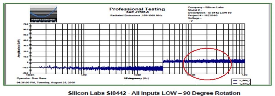
SKYWORKSSi8442のエミッションデータです。搬送波は数百MHzあたりですがエミッションの影響はみられません。
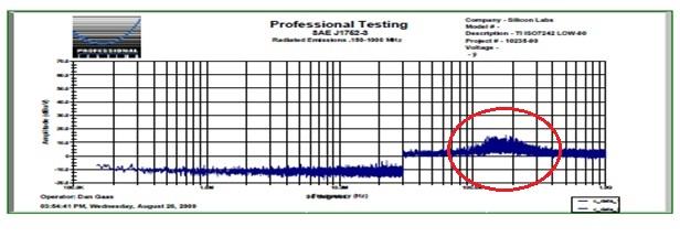
同じCAPACITIVE方式の他社データです。 搬送波と思われる周波数付近でエミッションが高くなっているように見えます。
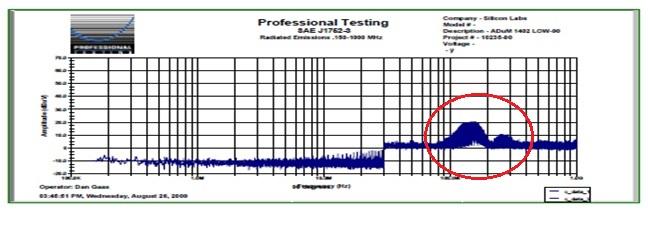
コイルベースで伝送する製品のデータです。搬送周波数と思われる付近のエミッションはより高い様です。
情報機器、医療機器 などのアプリケーションで低EMIの製品が求められます。
[参考資料]
Low EMI Isolation for Medical Equipment Applications
AN1131: Design Guide for Reducing Radiated and Conducted Emissions in Isolated Systems Using Skyworks’ Isolators
Isolator vs. Optocoupler Technology
消費電流と信号通信方式(OOK:On-Off-Keying vs エッジトリガー)の違い
各種アイソレーターの消費電流を比較しました。ここでは消費電流と信号通信方式(OOK:On-Off-Keying vs エッジトリガー)の違いに関して比較します。
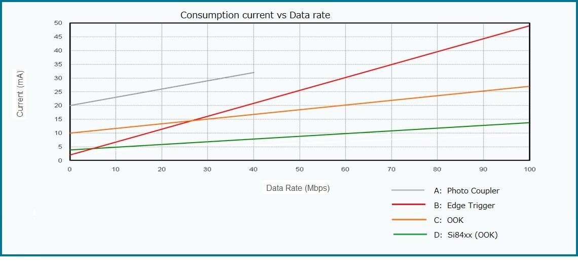
エッジトリガーの技術では、消費電流は入力側も出力側も入力の周波数に応じて上がります。そのため、入力の周波数が低い場合は、消費電流を下げることが可能です。
一方、OOK(On-Off-Keying)の1次側の回路電流は信号のデューティーに依存します。2次側は負荷や周波数に応じて電流は大きくなります。ON時は搬送波を送り続けるので消費電流は高くなりますがノイズに強いので車載製品、モーターなどの外乱ノイズの多いアプリケーションでは、OOKを用いた製品が主流となっています。SKYWORKSのアイソレーターは、OOKでありながら低消費電流でデータレートも150MHzと優れた製品があります。
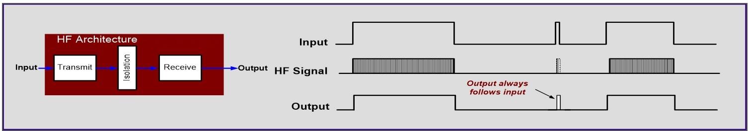
OOK(On-Off-Keying)方式は、入力がHigh(又はLow)の時だけ信号を送り続けることによって出力を制御します。フォトカプラーも同様の制御方法です。この方式の良い点は、たとえ外乱によって出力が変化してもすぐに復帰することです。SKYWORKS製品では更に消費電流を減らせる様、信号の偏りによってHigh/Lowどちらで搬送波を送るかのオプションを備えているものもあります。
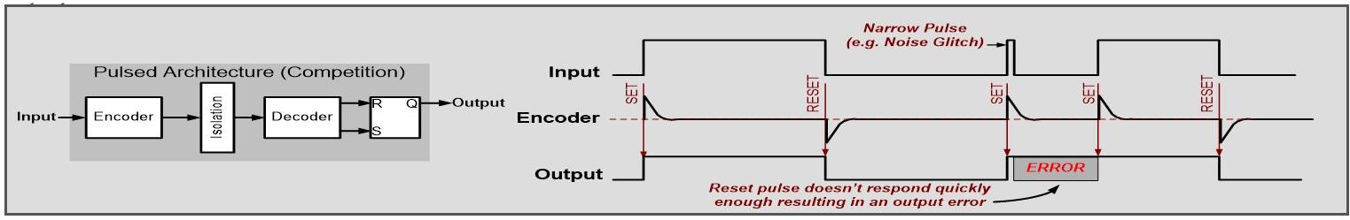
一方で、他社のデジタルアイソレーターでみられるエッジトリガー方式では、入力の遷移(H→L/L→H)をみて出力の状態を変化させます。消費電流は入力周波数に応じて変化するので、特に低速の信号通信をおこなう場合は、消費電流を下げることが可能です。遷移信号を正常に通信させるため、外乱が入らないようにフィルターを備えていますが、それでも外乱が入る可能性があり、左図のように出力が反転してしまうといった誤動作に繋がる可能性があります。定期的に入力側の状態信号を送ったり、立上がり/下がりエッジで違う信号を送るなど、一定の対策が施されているものもありますが、ノイズの多いアプリケーションでは注意が必要です。
電磁界の影響
各種アイソレーターについて電磁界の影響を比較しました。実機において電磁界は配線などに対しても影響をあたえるので、設計、評価の際は注意する必要があります。スタンダードなデジタルアイソレーター(Si84xxやSi86xxなど)は電磁界に対して強い耐性をもっており、電力メーターのTamper-Proofをサポートしています。これらは300V/mの電界に対する耐性 1000A/m以上の磁界に対して耐性をもっています。
磁界の影響
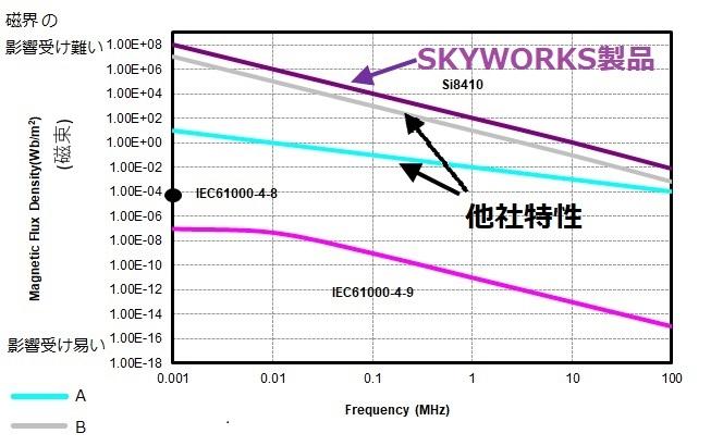
このグラフでは磁界(磁束)に対する影響を比較しています。各社 50 Hz/ 60 Hz の電源周波数磁界のイミュニティー試験IEC 61000-4-8や、パルス磁界イミュニティー試験IEC 61000-4-9などの測定規格で一定の特性をクリアできているようですが、中でもSkyworks製品の磁界に対する耐性は特に強い様です。
電界の影響
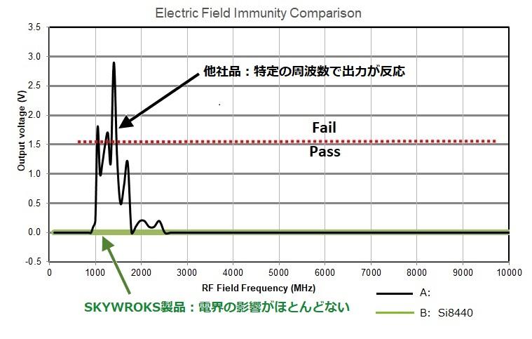
このグラフは電界を周波数を変えて与え、出力をモニターした結果です。SKYWORKS Si84xxでは10GHzまでの 300V/mの電界での影響はありませんでした。しかし、磁気結合方式のこの機種では1GHz(1000MHz)付近の電界に反応した様です。
車載品や大型動力機器などのアプリケーションでよくある大電流の流れるケーブルなどが、近くにある環境では電磁界に強い製品が求められます。
[参考資料]
Low EMI Isolation for Medical Equipment Applications
CMOS Digital Isolators Supersede Optocouplers in Industrial Applications
Isolator vs. Optocoupler Technology
まとめ
デジタルアイソレーターが世に出てから数十年が経過し、多くの製品で使用いただく様になりました。フォトカプラーより入出力の遅延時間が格段に短く、温度変化に対するばらつきが少ないという特性は、システムの効率をあげるのに欠かせない重要な役割を果たしています。
各種デジタルアイソレーター間でも容量絶縁と磁気絶縁という構造の違いや、OOK(On-Off-Keying)とエッジトリガーなどの通信方式の違いにより、上述したようなエミッション、消費電流等の差分があります。
SKYWORKS社のアイソレーターは 最も古くから生産されてきたデジタルアイソレーターの1つで非常に良い特性を持っています。絶縁素子をお探しの場合は、ぜひご検討ください。
製品紹介ページのご案内
上述したアーキテクチャー/特徴を持った、デジタルアイソレーターの製品紹介ページはこちらです。
お問い合わせ
本記事に関して質問などありましたら、以下よりお問い合わせください。
スカイワークス社 メーカー情報Topへ
スカイワークス社のメーカー情報Topページに戻りたい方は以下をクリックください。