- Semiconductor BusinessHOME
- Products and Services of Macnica,Inc.
-
technical information

-
Events and Seminars
- Handling Manufacturer
- Support
- Inquiry
- Click here to purchase products
- Semiconductor business e-mail magazine registration
![]()
![]() Narrow down by specifying conditions
Narrow down by specifying conditions
現在2183件がヒットしています。check

Performance required for operational amplifiers
In recent years, with the spread of IoT, we are about to enter an era in which society is connected by trillions of sensors (1 trillion sensors). Sensors are being installed for advanced control. Sensors are devices that convert environmental and physical changes into electrical signals, and applications that use sensors demand higher performance from operational amplifiers year by year.
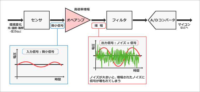
The diagram below shows the general flow of incorporating environmental and physical changes into the system.
The output of a sensor that converts weak environmental changes such as light, temperature, shock, and pressure into signals is often a minute analog signal. Required.
Are CMOS op amps noisy?
Although there are various types of operational amplifiers, the characteristics of the devices differ greatly depending on the configuration of the differential amplifier circuit in the input stage. The configuration of the input stage differential amplifier circuit is generally divided into three types: bipolar input, J-FET input, and CMOS input.
Bipolar op amps have the advantage of low noise, but the input bias current is large due to current drive. This is a disadvantage for amplifying high impedance sensors. On the other hand, although CMOS op amps have low input bias current and low power consumption, it is generally said that they have the disadvantage of high noise.
The table below compares the features of each. I compared the characteristics that are important to the sensor: input bias current, input offset voltage, noise (input equivalent noise voltage density), low voltage operation, and current consumption.
* Input conversion noise voltage density will be explained later.
| Input stage process | noise | input bias current |
offset Voltage |
Low voltage operation | current consumption |
| bipolar input | ○ | X | ○ | X | X |
| J-FET input | ○ | △ | △ | △ | X |
| CMOS input | X | ○ | △ | ○ | ○ |
○: good, X: bad, △: moderate
CMOS is best if the characteristics can be improved
A CMOS structure with a small input bias current is suitable for sensor amplifiers for high-impedance sensor elements, but the characteristics circled in red in the table are inferior. However, if the noise (input equivalent noise voltage density) and input offset voltage can be improved, it can be said that the op amp is suitable for sensors.
Noise countermeasures generated from operational amplifiers
To improve noise (input equivalent noise voltage density), we will first explain the types of noise. There are various types of noise, but they can be broadly classified into disturbance noise and noise generated by devices.
ノイズの分類
- Disturbance noise
Disturbance noise is electromagnetic waves emitted from the outside of the IC and radio waves (RF noise) emitted from electronic devices such as mobile phones and radios. As an aside, measures to prevent electromagnetic noise from being generated from electronic equipment are called EMI (emission) countermeasures, and measures to prevent electronic equipment from malfunctioning due to electromagnetic noise are called EMS (immunity) countermeasures.
- colored noise
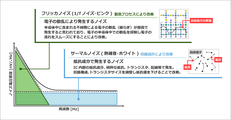
On the other hand, noise generated from devices such as transistors and resistors that make up an operational amplifier is called colored noise. Colored noise generated inside an operational amplifier includes frequency-dependent noise called pink noise (also known as 1/f noise, flicker noise) and white noise (also known as thermal noise) distributed uniformly over the entire frequency band. These two colored noises are expressed in the specs as input conversion noise voltage density.
Measures to reduce colored noise
The next step is to reduce the noise and colored noise generated by the device. We know the countermeasures according to the cause of noise generation.
- Flicker noise (1/f noise, pink noise)
Flicker noise (1/f noise/pink noise) caused by electron scattering can be improved through manufacturing processes. It is said to be caused by the scattering (fluctuation) of electrons due to impurities contained in the semiconductor, and it can be improved by suppressing the scattering of electrons in the semiconductor and smoothing the flow of electrons.
- Thermal noise (white noise)
Thermal noise (white noise) generated by resistance components can be improved by circuit design. The cause is that the electrons move erratically because resistance prevents the movement of charges. Since it occurs in the resistance component inside the IC, pure resistance, transistors, wiring, etc., it can be improved by adjusting the circuit configuration and transistor size to lower the resistance value.
Low noise operational amplifier LMR1802G-LB in spite of being CMOS
This time, I would like to introduce the operational amplifier LMR1802G-LB provided by ROHM.
This operational amplifier uses ROHM's unique circuit technology and process technology to achieve low noise in spite of being CMOS. The equivalent input noise voltage density, which indicates the noise generated by the device, achieves the same low noise performance as a bipolar low-noise operational amplifier.
| index/frequency | Equivalent Input Noise Voltage Density | |||
| LMR1802G | Conventional CMOS product | J-FETs | bipolar | |
| 1kHz | 2.9nV/√Hz | 19nV/√Hz | 7.2nV/√Hz | 4.2nV/√Hz |
| 10Hz | 7.8nV/√Hz | 38nV/√Hz | 9.0nV/√Hz | 5.0nV/√Hz |
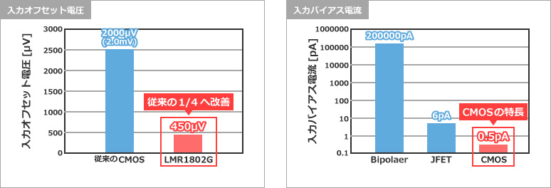
The input offset voltage has also been improved to 1/4 compared to conventional models.
In addition, the input offset voltage has also been improved to 1/4 that of conventional CMOS products.
Of course, the input bias current, which is a characteristic of CMOS op amps, is only 0.5 pA, making it an ideal product for sensors.
Can be used for various purposes other than sensors
The low noise operational amplifier LMR1802G-LB is compact and highly accurate, making it suitable for a wide variety of applications.
Application example
- industrial equipment
- Various sensor amplifiers
- battery powered equipment
- current sense amplifier
- ADC peripheral circuit, buffer amplifier
- Photodiode peripheral circuit
- Various amplifiers
| main important characteristics | spec |
| Input offset voltage | 5 μV (Typ) |
| Equivalent Input Noise Voltage Density | f=10Hz: 7.8nV/√Hz (Typ), f=1kHz: 2.9nV/√Hz (Typ) |
| Input common mode voltage range | VSS to VDD-1.0V |
| Input bias current | 0.5 pA (Typ) |
| Operating power supply voltage range | Single supply: 2.5 V to 5.5 V, dual supply: ±1.25 V to ±2.75 V |
| Operating temperature range | -40°C to +125°C |
| package W (Typ) x D (Typ) x H (Max) |
SSOP5, 2.90mm x 2.80mm x 1.25mm |